Method for measuring thickness of thin film-like material during surface polishing, and surface polishing method and surface polishing apparatus

a technology of thin film-like material and surface polishing method, which is applied in the direction of lapping machines, manufacturing tools, instruments, etc., can solve the problems of affecting the assembly micromachine and microsensor performance, affecting the flatness and parallelism of silicon wafers, and affecting the quality of an integrated circuit, so as to achieve accurate measurement, easy insertion and pulling out, and accurate performance

Active Publication Date: 2007-03-20
SUMITOMO MITSUBISHI SILICON CORP
View PDF6 Cites 36 Cited by
  • Summary
  • Abstract
  • Description
  • Claims
  • Application Information

AI Technical Summary

Benefits of technology

[0014]In view of the foregoing, it is an object of the invention to provide a thickness measuring method which can optically perform the measurement of the remaining film thickness of the thin film-like material such as the semiconductor wafer during surface polishing and the detection of the process finish point with high accuracy.
[0015]It is another object of the invention to provide the surface polishing method and the surface polishing apparatus which can polish the thin film-like material with high accuracy by adopting the thickness measuring method.

Problems solved by technology

Recently, demand for flatness and parallelism of the silicon wafer becomes more severe.
Accuracy of the thickness measurement largely affects a semiconductor device manufactured by the apparatus, which in turn affects quality of an integrated circuit.
At this point, the thickness of the SOI structure active layer largely affects the accuracy of dimension of the microfabrication, which in turn affects the assembled micromachine and performance of the microsensor.
However, all the conventional substrate polishing apparatuses are extensions of the existing apparatus, and currently the conventional substrate polishing apparatus does not sufficiently satisfy the upgrading demand for the accuracy of finishing.
Particularly the conventional management method performed by setting a machining time can not sufficiently deal with variations in remaining film thickness between lots.
However, the conventional management method performed by setting the machining time can not sufficiently deal with the variable factor of the polishing quantity per unit time.
However, in this method, the following drawback can be cited, in addition to a drawback that temporal stop of the polishing operation is required for the measurement.
Even if the correct remaining film thickness of the substrate which has been already polished is obtained to a certain extent by the measurement, it is still difficult to accurately obtain the remaining film thickness of a final target due to the above-described variable factors.
Since the method can not still solve the difficulty of obtaining accurately the remaining film thickness of the final target, a process finish point can not be accurately detected.
However, in the finish point detection methods which have been proposed, the discloser is limited to only a scope of principle, and an arrangement of constituents such as the specific optical system has not been clearly disclosed.
In this method, it is necessary that a monitor device is fixed to the rotating polishing surface plate, and the monitor device includes the light source and a photodetector, so that a considerable storage space for storing the monitor device is required in a lower portion of the polishing surface plate.
Consequently, there is a large constraint in design of the CMP polishing apparatus.
Therefore, the large storage space not only decreases a degree of freedom of the design but also becomes large obstacles of the miniaturization and the weight saving of the CMP polishing apparatus.
However, the surface polishing operation of the wafers having the different diameters causes trouble with replacement operation of the wafer holder.
Therefore, the replacement operation is not easy.

Method used


Image

  • Method for measuring thickness of thin film-like material during surface polishing, and surface polishing method and surface polishing apparatus
  • Method for measuring thickness of thin film-like material during surface polishing, and surface polishing method and surface polishing apparatus
  • Method for measuring thickness of thin film-like material during surface polishing, and surface polishing method and surface polishing apparatus

Examples


Embodiment Construction

[0064]The preferred embodiments of the invention will be described referring to the accompanying drawings.

[Surface Polishing Apparatus]

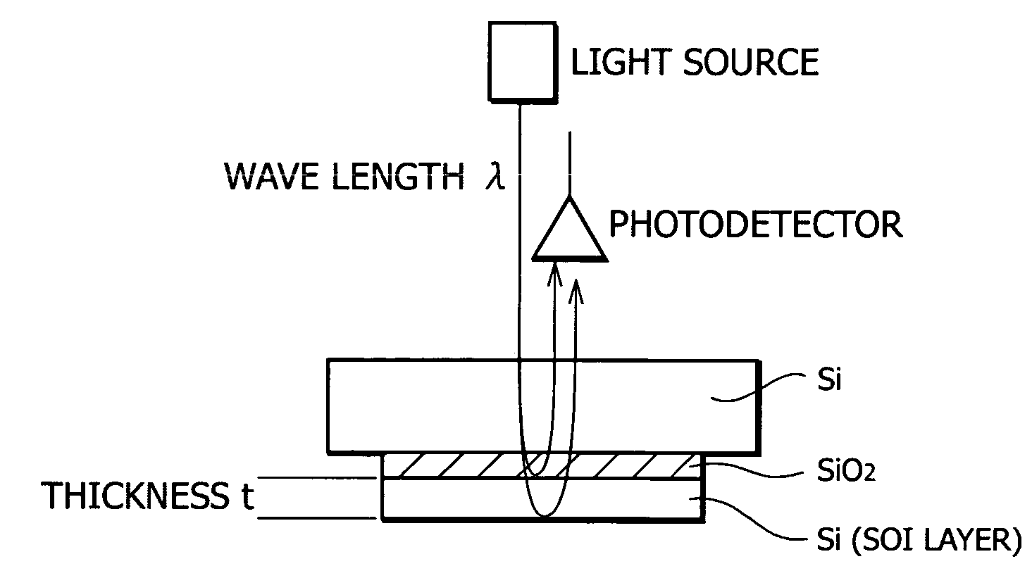
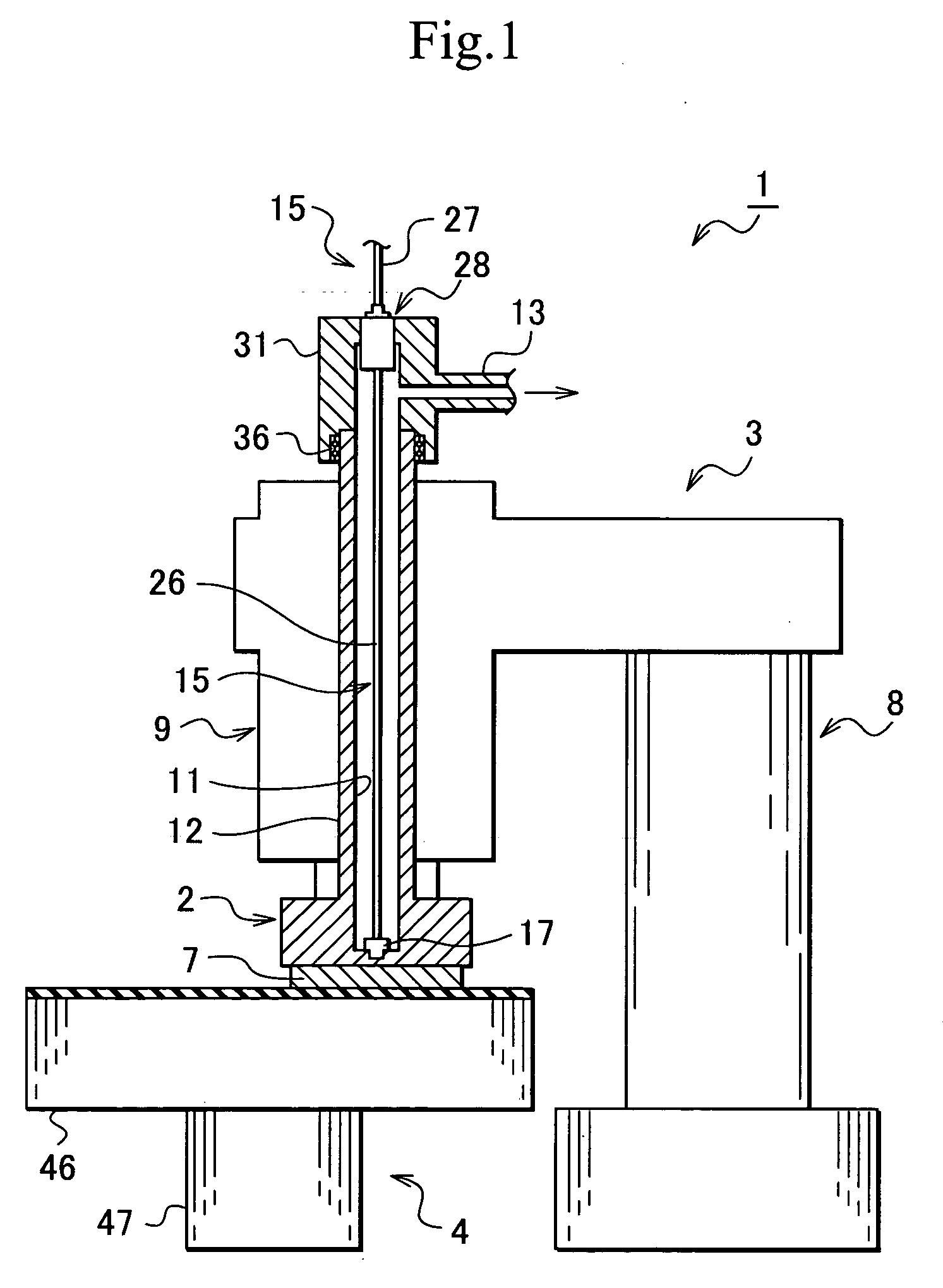
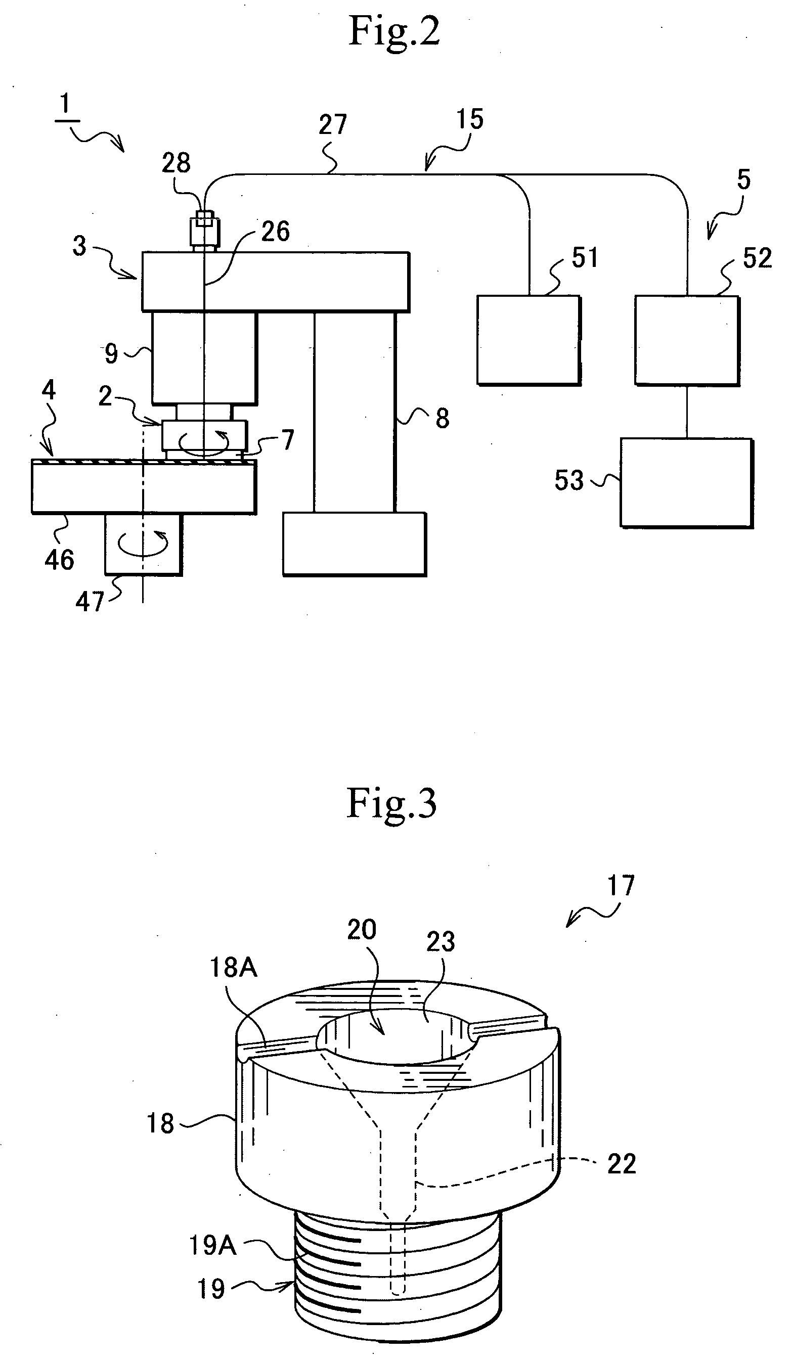
[0065]As shown in FIGS. 1 and 2, a surface polishing apparatus mainly includes a holder unit 2, a main body unit 3, a polishing surface plate 4, and a control unit 5.

[0066]The holder unit 2 holds a wafer 7 which is of the thin film-like material to be polished. The holder unit 2 is rotatably supported downward at a lower end of a rotation support unit 9 of the main body 3 mentioned later. The lower surface of the holder unit 2 is one which sucks the wafer 7. Specifically, a plurality of suction ports (not shown) for evacuation is provided in the lower surface of the holder unit 2.

[0067]The main body unit 3 rotatably supports the holder unit 2 and drives rotation of the holder unit 2 at the setting number of revolutions during the polishing. The main body unit 3 includes a base unit 8 and the rotation support unit 9. The base unit 8 is fixed to a floo...


PUM


Abstract

A thickness of a wafer during polishing operation is detected to accurately perform the polishing. A thickness measuring method, which measures the thickness of the wafer of wafer 7 in polishing a surface, comprises the steps of irradiating the thin film-like material during the surface polishing from a backside with probe light, measuring a reflectance spectrum with a dispersion type multi-channel spectroscope using a photodiode array which has particularly high sensitivity to light having a wavelength ranging from 1 to 2.4 μm, and calculating the thickness on the basis of a wave form of the reflectance spectrum. The surface polishing is performed while the thickness of the wafer 7 is measured by the above-described thickness measuring method, and the polishing is finished when the thickness of the wafer 7 reaches a target thickness.

Description

CROSS-REFERENCE TO RELATED APPLICATION[0001]This application claims, under 35 USC 119, priority of Japanese Application No. 2003-186245 filed Jun. 30, 2003.BACKGROUND OF THE INVENTION[0002]The present invention relates to a thickness measuring method used in polishing a surface of a thin film-like material such as a semiconductor wafer, and a surface polishing method and a surface polishing apparatus. Specifically, the invention relates to the method of measuring a thickness of the thin film-like material during the surface polishing, which measures and controls the thickness of the thin film-like material while performing the polishing process in polishing the thin film-like material such as an active layer surface of SOI (Silicon On Insulator) or a silicon wafer surface, and a surface polishing method and a surface polishing apparatus.[0003]After a slicing process, the silicon wafer is mirror-polished in the polishing process through a rapping process and an etching process. The t...

Claims


Application Information

Patent Timeline
Patent Type & Authority Patents(United States)
IPC IPC(8): G01B9/02B24B37/013B24B49/02G01B11/06B24B49/12H01L21/304
CPCB24B49/12B24B37/013
Inventor ISEI, YOSHITOHIRAI, TOKUMI
Owner SUMITOMO MITSUBISHI SILICON CORP
Why Eureka
Try Eureka