
Methods and apparatus for packaging integrated circuit devices

a technology of integrated circuit devices and packaging dies, applied in electrical equipment, semiconductor devices, semiconductor/solid-state device details, etc., can solve the problems of poor bond formation of bonding and tabs, high temperature and mechanical pressure on dies, and problems such as the problem of wire bonding and tab technology

Active Publication Date: 2007-03-20
TESSERA TECH HUNGARY KFT +1
View PDF93 Cites 90 Cited by
  • Summary
  • Abstract
  • Description
  • Claims
  • Application Information

AI Technical Summary

Benefits of technology

This approach results in a compact, environmentally protected, and mechanically strengthened integrated circuit package that allows for efficient electrical connection and thermal management, enabling the use of a wider range of substrates and reducing packaging size while maintaining high reliability.

Problems solved by technology

Both wire bonding and TAB bonding are prone to bad bond formation and subject the die to relatively high temperatures and mechanical pressures.
Both wire bond and TAB technologies are problematic from a package size viewpoint, producing integrated circuit devices having a die-to-package area ratio ranging from about 10% to 60%.
The flip-chip does not provide packaging but rather only interconnection.
The interconnection encounters problems of uniformity in the solder balls as well as in thermal expansion mismatching, which limits available substrates to silicon or to materials which have thermal expansion characteristics similar to those of silicon.

Method used


Image

  • Methods and apparatus for packaging integrated circuit devices
  • Methods and apparatus for packaging integrated circuit devices
  • Methods and apparatus for packaging integrated circuit devices

Examples


Embodiment Construction

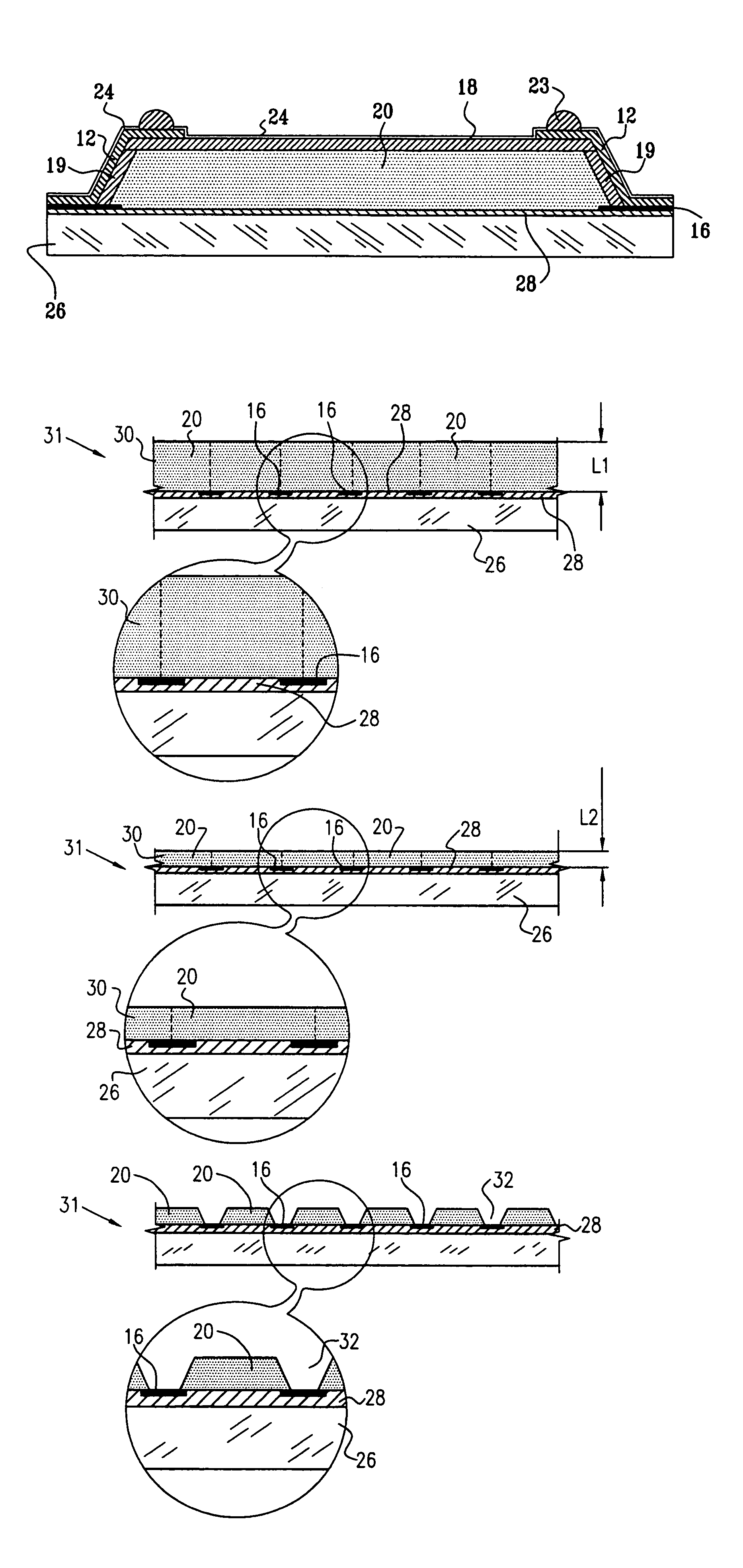
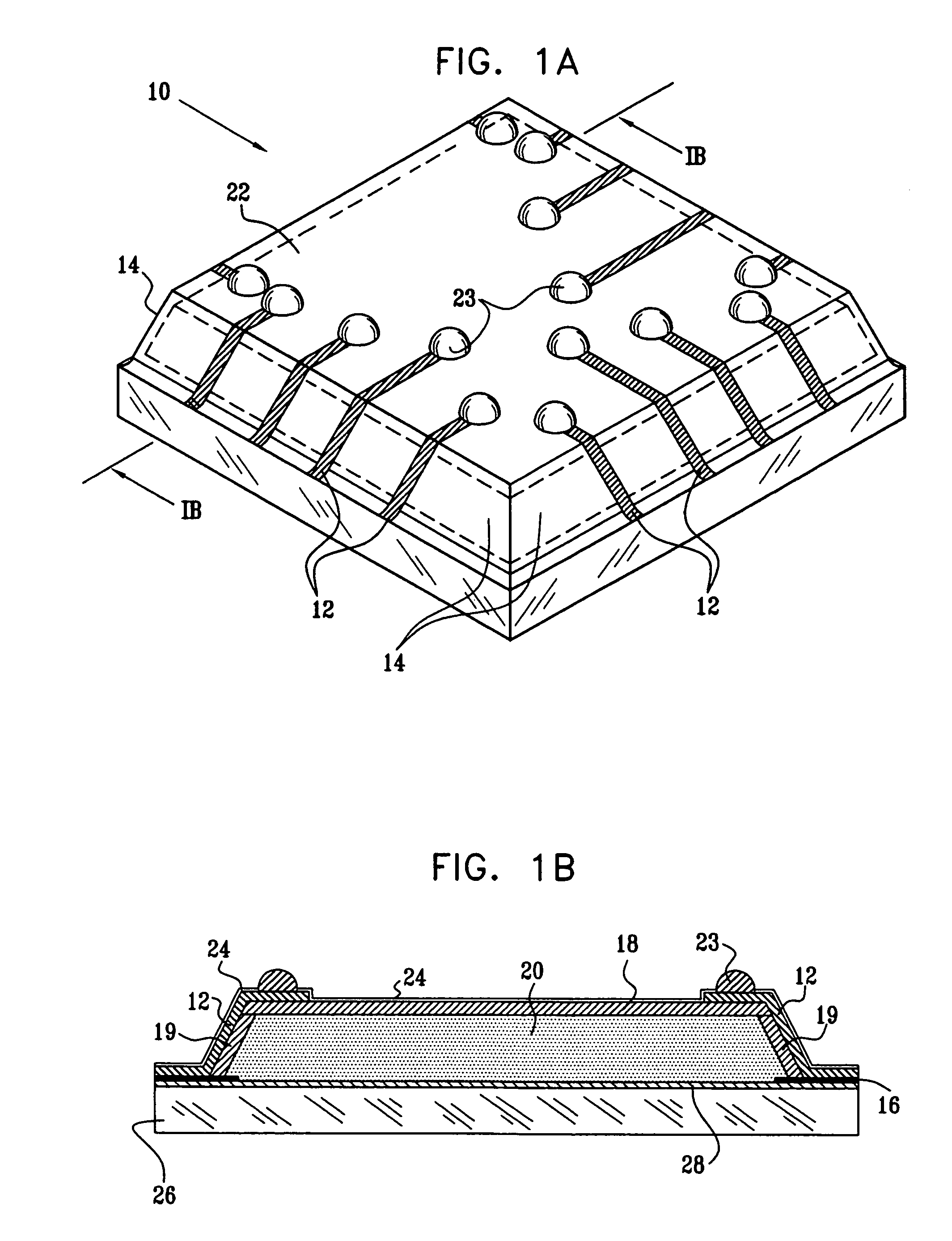
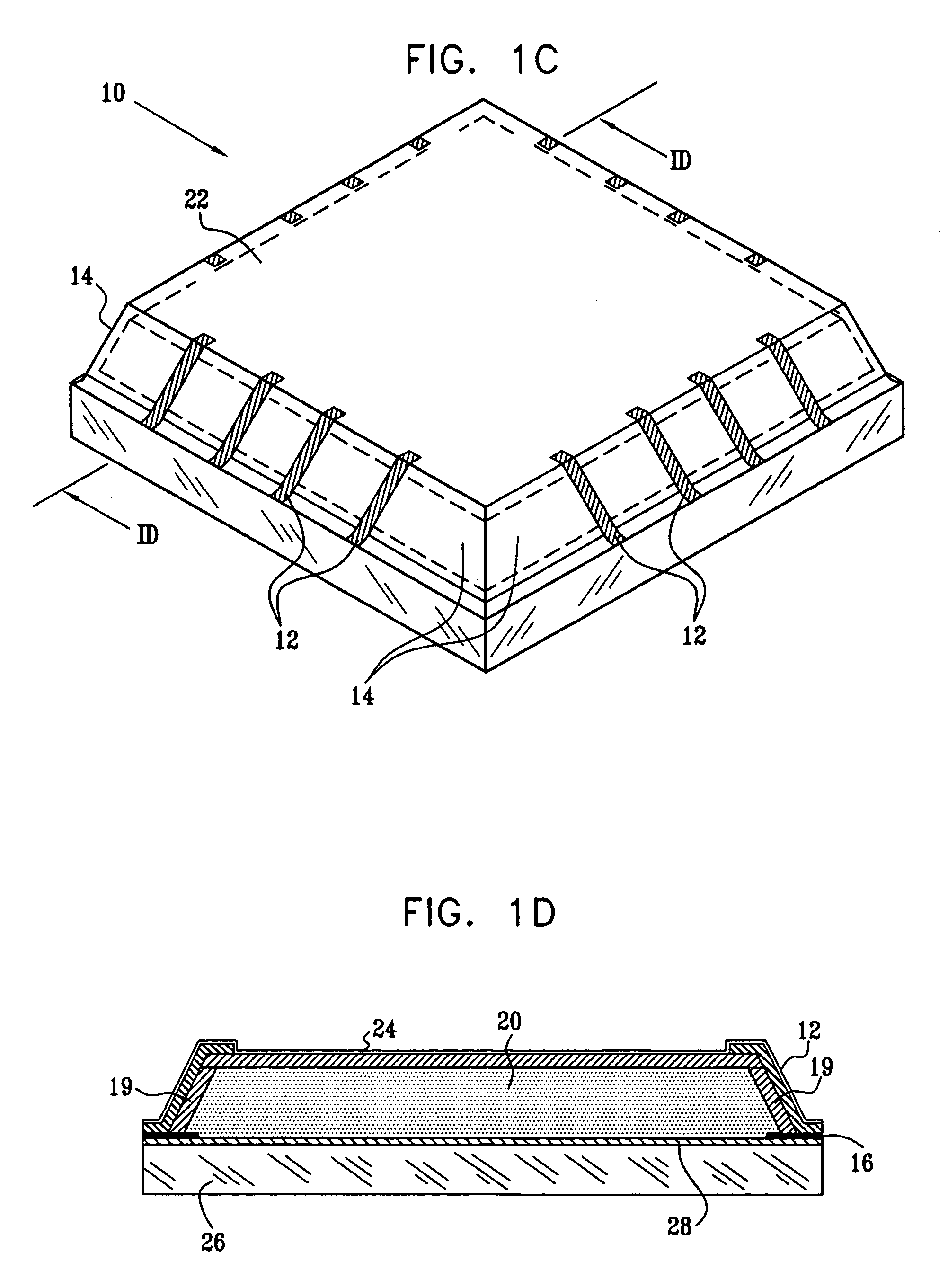
[0087]Reference is now made to FIGS. 1A–3J, which illustrate integrated circuit devices, preferably optronic, integrated circuit devices, and the production thereof, in accordance with a preferred embodiment of the present invention. As seen in FIGS. 1A and 1B, the integrated circuit device includes a relatively thin and compact, environmentally protected and mechanically strengthened, integrated circuit package 10, preferably an optronic integrated circuit package, having a multiplicity of electrical conductors 12 plated along the edge surfaces 14 thereof.

[0088]It is a particular feature of the present invention that conductors 12 are electrically connected to pads 16, and preferably are formed directly over insulation layers 18 and 19 overlying a die 20, without there being an intervening packaging layer, such as a glass layer. Insulation layers 18 and 19 may each comprise one or more layers such as dielectric layers and / or passivation layers and may be different from each other i...


PUM


Abstract

An integrally packaged integrated circuit device including an integrated circuit die including a crystalline substrate having first and second generally planar surfaces and edge surfaces and semiconductor circuitry formed over the first generally planar surface, at least one chip scale packaging layer formed over the semiconductor circuitry and the first generally planar surface, an insulation layer formed over the second generally planar surface and the edge surfaces and at least one electrical conductor formed directly on the insulation layer overlying the second generally planar surface, the at least one electrical conductor being connected to the circuitry by at least one pad formed directly on the first generally planar surface.

Description

FIELD OF THE INVENTION[0001]The present invention relates to methods and apparatus for producing integrated circuit devices and to integrated circuit devices produced thereby and more particularly to an integrally packaged die.BACKGROUND OF THE INVENTION[0002]An essential step in the manufacture of all integrated circuit devices is known as “packaging” and involves mechanical and environmental protection of a silicon chip that is at the heart of the integrated circuit as well as electrical interconnection between predetermined locations on the silicon chip and external electrical terminals.[0003]At present three principal technologies are employed for packaging semiconductors: wire bonding, tape automatic bonding (TAB) and flip chip.[0004]Wire bonding employs heat and ultrasonic energy to weld gold bonding wires between bond pads on the chip and contacts on the package.[0005]Tape automatic bonding (TAB) employs a copper foil tape instead of bonding wire. The copper foil tape is conf...

Claims


Application Information

Patent Timeline
Patent Type & Authority Patents(United States)
IPC IPC(8): H01L21/44H01L21/48H01L21/50H01LH01L23/06H01L23/31H01L31/0203H01L31/0232H01L33/48H01L33/62
CPCH01L27/14618H01L27/14621H01L27/14632H01L27/14683H01L27/14685H01L27/14687H01L31/0203H01L31/0232H01L33/385H01L24/11H01L23/3114H01L2224/0401H01L33/486H01L33/62H01L2224/0231H01L2224/1147H01L2224/13099H01L2924/01013H01L2924/01022H01L2924/01029H01L2924/01033H01L2924/01047H01L2924/01057H01L2924/01074H01L2924/01077H01L2924/01078H01L2924/01079H01L2924/01082H01L2924/14H01L2924/01006H01L2924/01024H01L2924/014H01L2924/10253H01L2924/00H01L24/02H01L24/05H01L24/13H01L31/02327H01L2224/0236H01L2224/02377H01L2224/05548H01L2224/05624H01L2224/05647H01L2224/05666H01L2224/05671H01L2224/0616H01L2224/13024H01L2924/0001H01L2924/00014H01L2924/013H01L2224/02H01L23/28H01L23/52
Inventor ZILBER, GILAKSENTON, JULIAOGANESIAN, VAGE
Owner TESSERA TECH HUNGARY KFT
Learn More