Electronic component with bump electrodes, and manufacturing method thereof

a manufacturing method and technology of bump electrodes, applied in the direction of final product manufacturing, sustainable manufacturing/processing, semiconductor/solid-state device details, etc., can solve the problems of difficult to manufacture electronic components with bump electrodes at an adequate yield, difficult to manufacture electronic components with bump electrodes at a high yield, and considerable time required to form such an electroless plating layer. , to achieve the effect of appropriately reducing the occurrence of open defects in the manufacturing process

Inactive Publication Date: 2007-03-13
FUJITSU LTD
View PDF13 Cites 28 Cited by
  • Summary
  • Abstract
  • Description
  • Claims
  • Application Information

AI Technical Summary

Benefits of technology

[0012]An object of the present invention, which was devised in view of this situation, is to provide an electronic component with bump electrodes that comprises a surface-protecting insulating film of adequate thickness and bump elements of adequate height, and allows the occurrence of open defects in the manufacturing process to be appropriately reduced; and to provide a manufacturing method thereof.

Problems solved by technology

For this reason, current-carrying layers for performing electroplating must be formed, removed by etching, or the like on the surface-protecting insulating film in accordance with this technique, making it difficult to manufacture electronic components with bump electrodes at an adequate yield.
The electroless plating layer must be formed until it becomes level with the surface of the insulating film in order to form adequate electroplated bump elements, and considerable time is required to form such an electroless plating layer.
It is therefore difficult to manufacture electronic components with bump electrodes at a high yield by means of the technology disclosed in the above application.

Method used


Image

  • Electronic component with bump electrodes, and manufacturing method thereof
  • Electronic component with bump electrodes, and manufacturing method thereof
  • Electronic component with bump electrodes, and manufacturing method thereof

Examples


##ventive example 1

Inventive Example 1

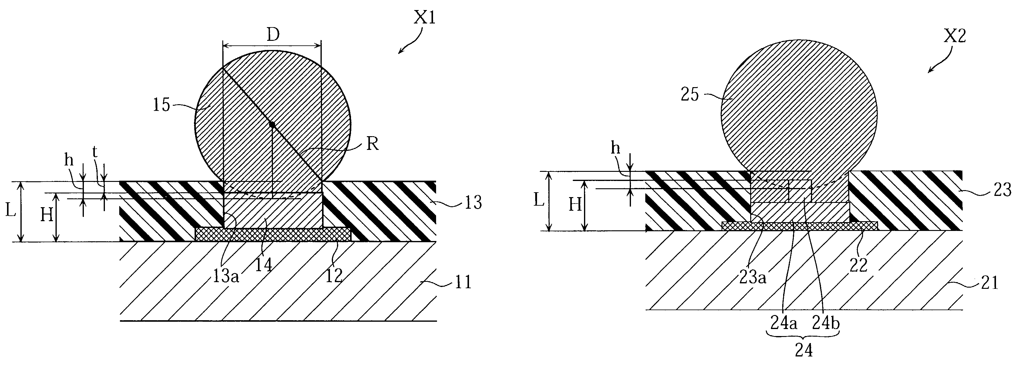
[0088]An epoxy acrylate resin film was formed by screen printing as an insulating film having photosensitivity so as to cover the electrode pads on the surface of a wiring board having Cu electrode pads (electrode diameter: 110 μm; electrode pitch: 220 μm; number of electrodes: 3000). The film thickness was set to 30 μm. An exposure treatment and a subsequent developing treatment were then performed on the insulating film, and a plurality of openings with a diameter of 90 μm was formed so as to expose each electrode pad. A 1.0% aqueous solution of sodium carbonate (Na2CO3) was used as the developing solution for the developing treatment. An Ni plating layer with a thickness of 15 μm was subsequently formed by electroless plating on the electrode pads of the openings. An Au plating layer with a thickness of 0.1 μm was then formed by electroless plating on the Ni plating layer. Electroconductive connecting elements comprising an Ni plating layer and an Au plating la...

##ventive example 2

Inventive Example 2

[0090]An epoxy acrylate resin film was formed by screen printing as an insulating film having photosensitivity so as to cover the electrode pads on the surface of a semiconductor chip having Cu electrode pads (electrode diameter: 90 μm; electrode pitch: 220 μm; number of electrodes: 3000). The film thickness was set to 10 μm. An exposure treatment and a subsequent developing treatment were then performed on the insulating film, and a plurality of openings with a diameter of 70 μm was formed so as to expose each electrode pad. A 1% aqueous solution of tetramethylammonium hydroxide (TMAH) was used as the developing solution for the developing treatment. An Ni plating layer with a thickness of 3 μm was subsequently formed by electroless plating on the electrode pads of the openings. An Au plating layer with a thickness of 0.1 μm was then formed by electroless plating on the Ni plating layer. Electroconductive connecting elements comprising an Ni plating layer and an ...

##ventive example 3

Inventive Example 3

[0092]The same wiring board as in Inventive Example 1 was prepared by the same steps as in Inventive Example 1 up to the formation of openings with a diameter of 200 μm in the photosensitive acrylate resin film, and flux was applied to the electrode pads exposed in the openings of the resin film in the wiring board. Solder balls (Sn-3.5% Ag solder) with a diameter of 130 μm were then placed on the electrode pads coated with the flux. A bump element was subsequently formed from the solder ball in each opening by conducting a heating treatment at a maximum temperature of 240° C. The acrylate resin film was then removed using a 5% monoethanolamine aqueous solution as an alkali stripping solution. As a result of these steps, it was possible to obtain a wiring board that had bump electrodes based on bump elements whose height from the insulating film was 110 μm and whose height nonuniformity was 2 μm.


PUM

PropertyMeasurementUnit
diameteraaaaaaaaaa
diameteraaaaaaaaaa
thicknessaaaaaaaaaa

Abstract

An electronic component with bump electrodes includes a surface-protecting insulating film of adequate thickness and bump elements of adequate height, and allows the occurrence of open defects in the manufacturing process to be appropriately reduced. An electronic component with bump electrodes (X1) includes a substrate (11), electrode pads (12) provided on the substrate (11), an insulating film (13) that has openings (13a) in correspondence with the electrode pads (12) and is laminated and formed on the substrate (11), electroconductive connecting elements (14) provided on the electrode pads (12) in the openings (13a), and bump elements (15) that are in direct contact with the electroconductive connecting elements (14) and project from the openings (13a).

Description

BACKGROUND OF THE INVENTION[0001]1. Field of the Invention[0002]The present invention relates to an electronic component with bump electrodes, and to a manufacturing method thereof. More particularly, the present invention relates to a semiconductor chip, printed wiring board, or other electronic component with bump electrodes such as a ball grid array (BGA), and to a manufacturing method thereof.[0003]2. Description of the Related Art[0004]The need for higher density in the packaging of electronic components on printed wiring boards, ceramic boards, and the like has increased in recent years, and bare chip packaging has attracted attention as a technology that satisfies this need. In bare chip packaging, the trend is in the direction of adopting face-down mounting or flip-chip bonding, which is accomplished by interposing bumps between a semiconductor chip and the electrode pads of a wiring board, instead of using the conventional face-up mounting, which is accomplished by wire bon...

Claims


Application Information

Patent Timeline
Patent Type & Authority Patents(United States)
IPC IPC(8): H05K1/11H01R12/04H01R9/00H05K3/00H01L21/60H01L23/485H05K3/24H05K3/34H05K7/10
CPCH01L24/11H05K1/111H05K3/243H05K7/1061H01L24/12Y10T29/49147H01L2224/05557H01L2224/05567H01L2224/1147H01L2224/13022H01L2224/13099H01L2924/01004H01L2924/01011H01L2924/01013H01L2924/01022H01L2924/01029H01L2924/0103H01L2924/01046H01L2924/01047H01L2924/01049H01L2924/01051H01L2924/01078H01L2924/01079H01L2924/01082H05K3/3452H05K3/3473H05K3/3478H05K2201/09736H05K2203/043H05K2203/0568H05K2203/0571H05K2203/0577H01L2224/13005H01L2224/05541H01L2224/05571H01L2224/13109H01L2924/01005H01L2924/01006H01L2924/01023H01L2924/01033H01L2924/014Y10T29/49149H01L2924/0002H01L2224/11334H01L2224/81191H01L2224/73204H01L2224/32225H01L2224/16225H01L2224/0401H01L2224/11902H01L2224/13006H01L2924/207H01L2924/00H01L2924/00012H01L2224/05552H01L24/03H01L24/05H01L2224/05147H01L2224/05609H01L2224/05611H01L2224/05613H01L2224/05616H01L2224/05618H01L2224/0562H01L2224/05624H01L2224/05639H01L2224/05644H01L2224/05647H01L2224/05655H01L2224/05664H01L2224/05666H01L2924/12042H01L2924/15787Y02P70/50H01L2924/00014H01L2924/013
Inventor SAKUYAMA, SEIKI
Owner FUJITSU LTD
Why Eureka
Try Eureka