Eureka AIR delivers breakthrough ideas for toughest innovation challenges, trusted by R&D personnel around the world.

Stackable electronic assembly

a technology of electronic assemblies and components, applied in the direction of electrical apparatus, semiconductor devices, semiconductor/solid-state device details, etc., can solve the problems of thermal cracking of solder points, electrical discontinuities, and solder points between them to crack, so as to reduce thermal cracking of soldered points, improve heat dissipation, and increase the memory capacity of the module

Inactive Publication Date: 2007-02-20
SANMINA-SCI CORPORATION
View PDF89 Cites 101 Cited by
  • Summary
  • Abstract
  • Description
  • Claims
  • Application Information

AI Technical Summary

Benefits of technology

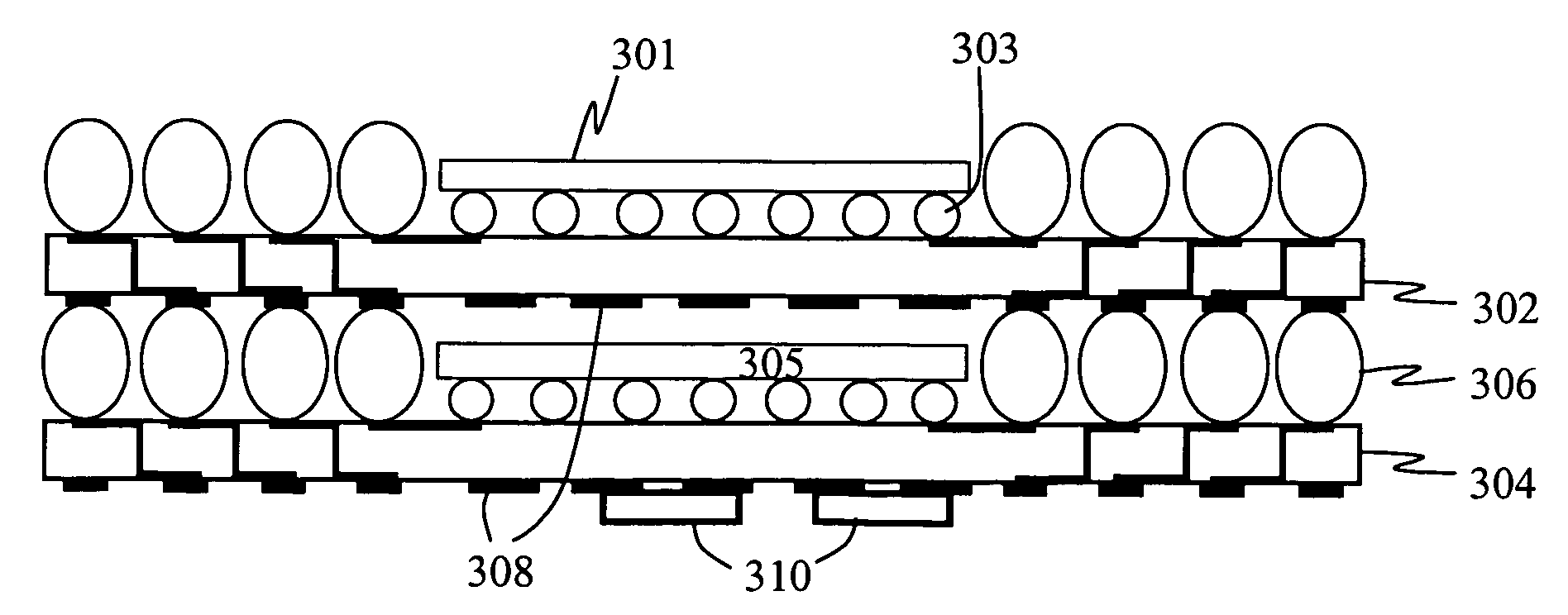
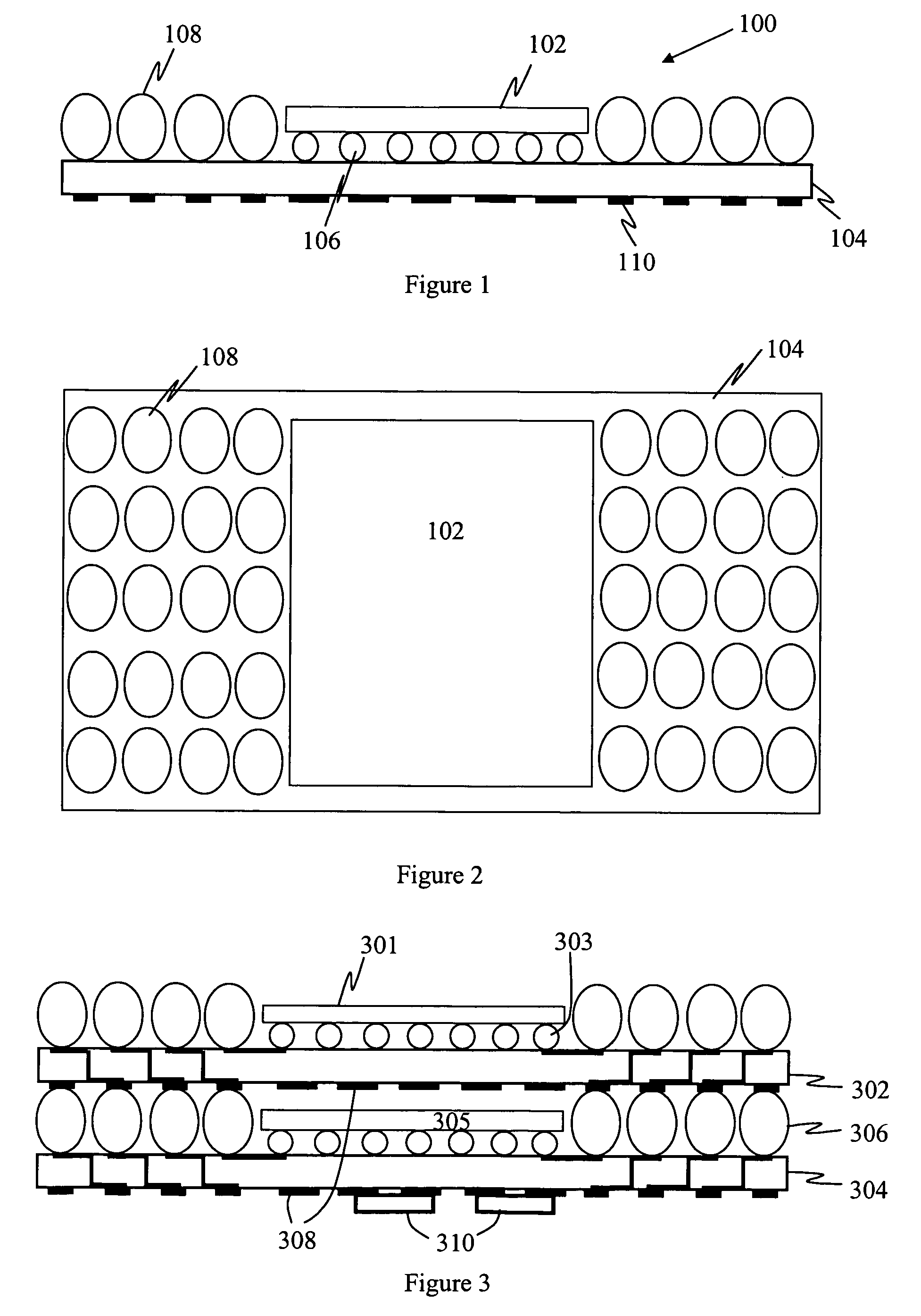
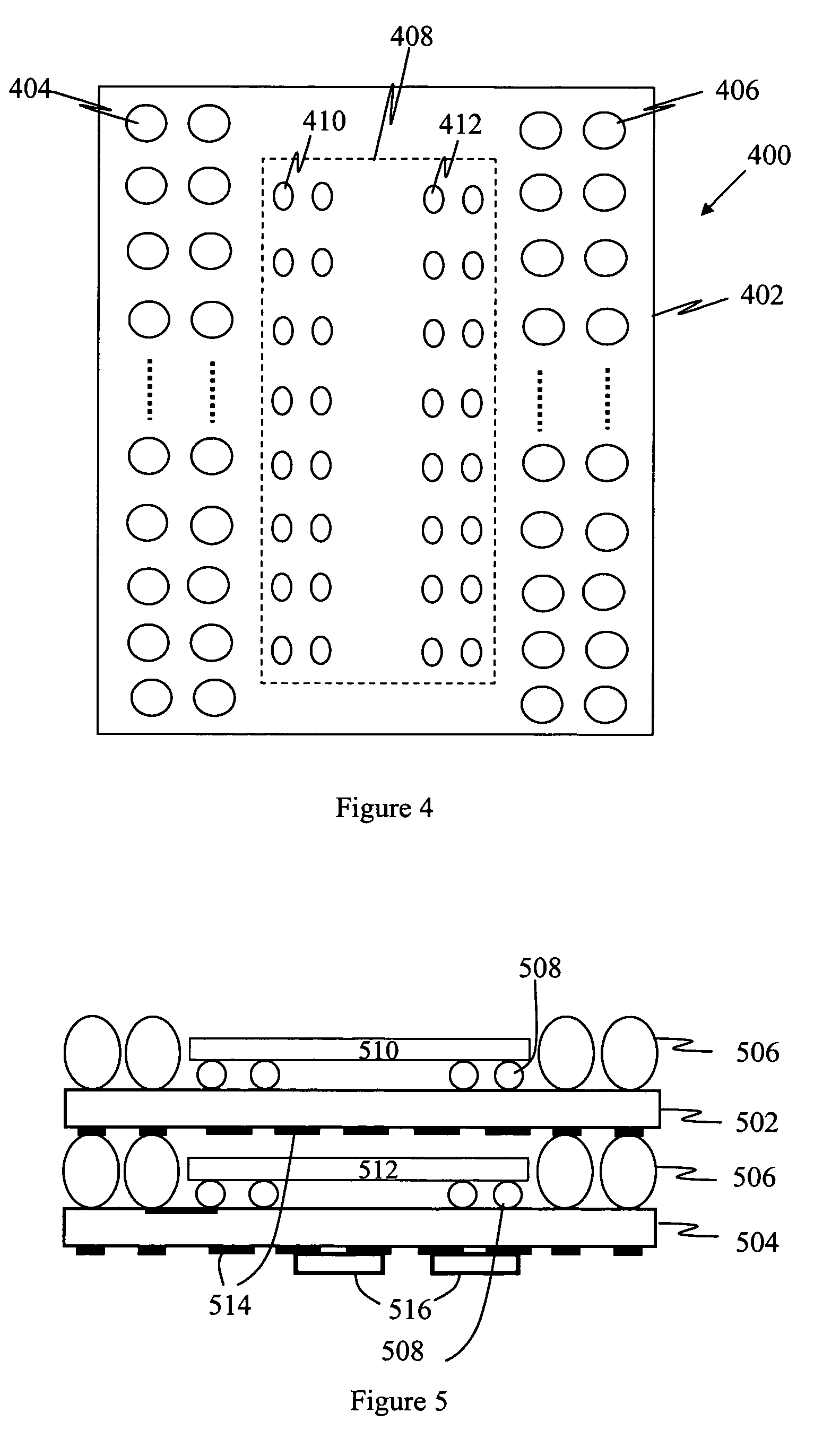
[0010]One aspect of the invention provides a stackable semiconductor device architecture with each semiconductor device soldered onto a chip-scale ball grid array package. A second aspect of the invention provides a way to reduce thermal cracking of soldered points by using controlled thermal expansion substrates that substantially match the coefficient of expansion of semiconductor devices mounted thereon. A third aspect of the invention provides a semiconductor die mounting technique that improves heat dissipation by exposing all six surfaces of the semiconductor die mounted on a chip-scale package. A fourth aspect of the invention provides a chip-scale ball grid array package that permits mounting of components, such as capacitors and resistors, thereon. A fifth aspect the invention provides a staggered routing scheme that enables the use of the same trace routing at every level of the stacked architecture.
[0011]One implementation of the invention provides a memory module with stacked chip-scale ball grid array packages that increase the memory capacity of the module, while conforming to module dimensional requirements.

Problems solved by technology

Thermal cracking may occur when the differences between the thermal coefficients of expansion for two materials causes solder points between them to crack.
For instance, if a semiconductor die was directly soldered onto a substrate having a substantially different coefficient of expansion, temperature cycling may eventually cause soldered points, such as solder balls, to crack thus causing an electrical discontinuities.
Additionally, semiconductor dice are typically quite fragile, sensitive to physical impact, and environmental conditions.
However, both underfilling and / or encapsulating a device or die increases the heat retained by the device.
Thus, the increase in temperature resulting from underfilling and / or encapsulation is an undesirable side effect of increasing the reliability by protecting an electronic device.
However, the number of memory components that may be placed on a substrate is limited by the size of the module.
Thus, the storage capacity of a memory module is often limited by physical size restrictions.
In particular, the surface area available on the memory module limits the number of memory components that can be mounted thereon.
However, the number of memory components that may be stacked is limited by the height restrictions on the memory module as well as the complexities of accessing stacked memory devices using existing bus interfaces designed for non-stacked architectures.

Method used


Image

  • Stackable electronic assembly
  • Stackable electronic assembly
  • Stackable electronic assembly

Examples


Embodiment Construction

[0020]In the following description numerous specific details are set forth in order to provide a thorough understanding of the invention. However, one skilled in the art would recognize that the invention may be practiced without these specific details. In other instances, well known methods, procedures, and / or components have not been described in detail so as not to unnecessarily obscure aspects of the invention.

[0021]In the following description, certain terminology is used to describe certain features of one or more embodiments of the invention. For instance, “die” refers to a semiconductor device, such as a silicon memory device, that is not packaged or covered in a protective plastic, epoxy, or other material. The term “underside coupling members” is used to refer to such relatively rigid electrical coupling members as conductive bumps, conductive balls (e.g., solder or gold balls), and conductive rods.

[0022]One aspect of the invention provides a stackable semiconductor device...


PUM


Abstract

On implementation of the invention provides a stackable chip-scale package for improving memory density that may be mounted within a limited area or module. A novel staggered routing scheme enables the use of the same trace routing at every level of the stacked architecture for efficiently accessing individual memory devices in a chip-scale package stack. The use of a ball grid array chip-scale package architecture in combination with thermally compatible materials decreases the risk of thermal cracking while improving heat dissipation. Moreover, this architecture permits mounting support components, such as capacitors and resistors, on the chip-scale package.

Description

FIELD[0001]Various embodiments of the invention pertain to stackable electronic assemblies. At least one embodiment of the invention pertains to a memory module using these stackable assemblies that enables higher memory densities.DESCRIPTION OF RELATED ART[0002]Semiconductor dice, such as memory dice, are often packaged for protection and ease of use. One type of package is a ball grid array package (BGA) in which a semiconductor die is mounted on a substrate. The semiconductor die has a plurality of bond pads that are electrically connected, via wires bonded between the metal traces on the substrate and on the die. The traces on the substrate terminate at contact pads where conductive elements, such as solder balls, are attached. The BGA package can then be mounted on a circuit board and electrically connected via the conductive elements. The BGA package may be electrically connected to metal traces on the circuit board in various ways, including applying heat or ultrasound to the...

Claims


Application Information

Patent Timeline
Patent Type & Authority Patents(United States)
IPC IPC(8): H01L23/02H01L23/498H01L25/065
CPCH01L23/49816H01L25/105H01L2224/16225H01L23/50H01L24/16H01L2225/06517H01L2225/0652H01L2225/06541H01L2225/06572H01L2924/01079H01L2924/10253H01L2924/15192H01L2924/15311H01L2924/1532H01L2924/15331H01L2924/19041H01L2924/19043H01L2924/19105H01L2924/19106H01L2924/3511H01L2225/1023H01L2225/1058H01L23/49838H01L23/12
Inventor ELLSBERRY, MARKSCHMITZ, CHARLES E.CHEN, CHI SHEALLISON, VICTOR
Owner SANMINA-SCI CORPORATION
Why Eureka
Eureka Blog
Learn More