Reactive sputtering of silicon nitride films by RF supported DC magnetron

a technology of dc magnetron and rf support, which is applied in the direction of electrolysis components, vacuum evaporation coatings, coatings, etc., can solve the problems of spikes, defects in film deposited, and circuitry on the chips has become progressively complex

Active Publication Date: 2007-02-20
OEM GRP LLC
View PDF8 Cites 17 Cited by
  • Summary
  • Abstract
  • Description
  • Claims
  • Application Information

AI Technical Summary

Problems solved by technology

Even as the chips have decreased in size, the circuitry on the chips has become progressively complex.
If the proper impedance values are not maintained, the operation of the electrical circuitry in the integrated circuit chip is impaired.
Moreover, the spike creates particles and defects in the film deposited on the substrate.

Method used


Image

  • Reactive sputtering of silicon nitride films by RF supported DC magnetron
  • Reactive sputtering of silicon nitride films by RF supported DC magnetron
  • Reactive sputtering of silicon nitride films by RF supported DC magnetron

Examples


Embodiment Construction

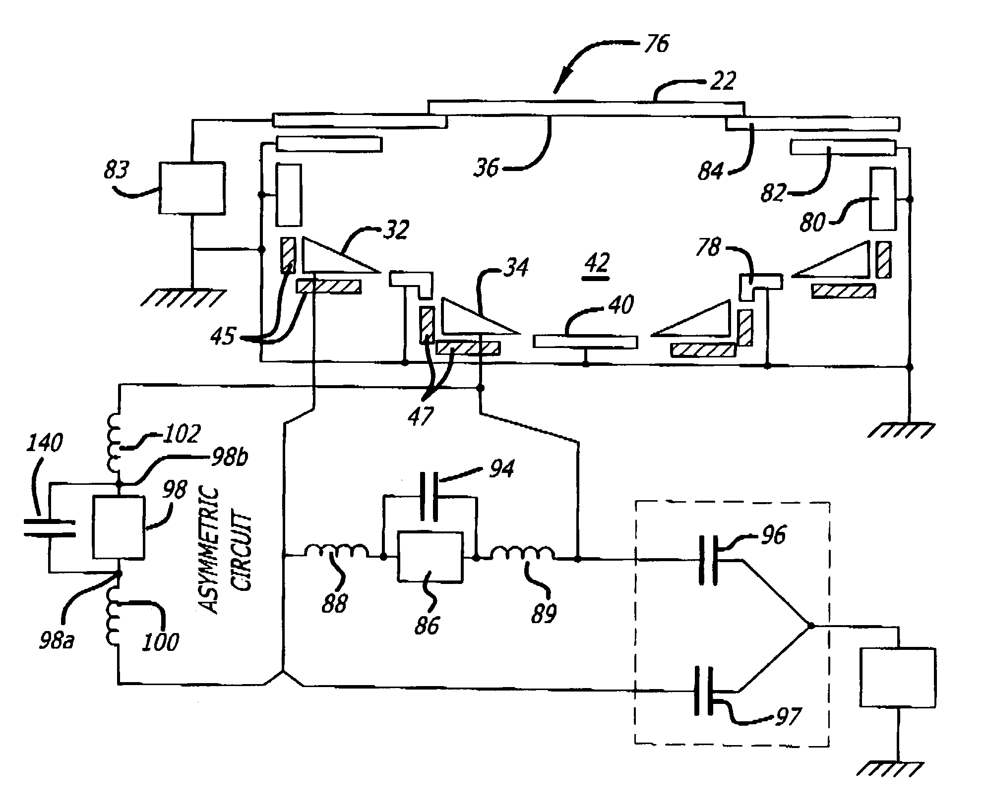
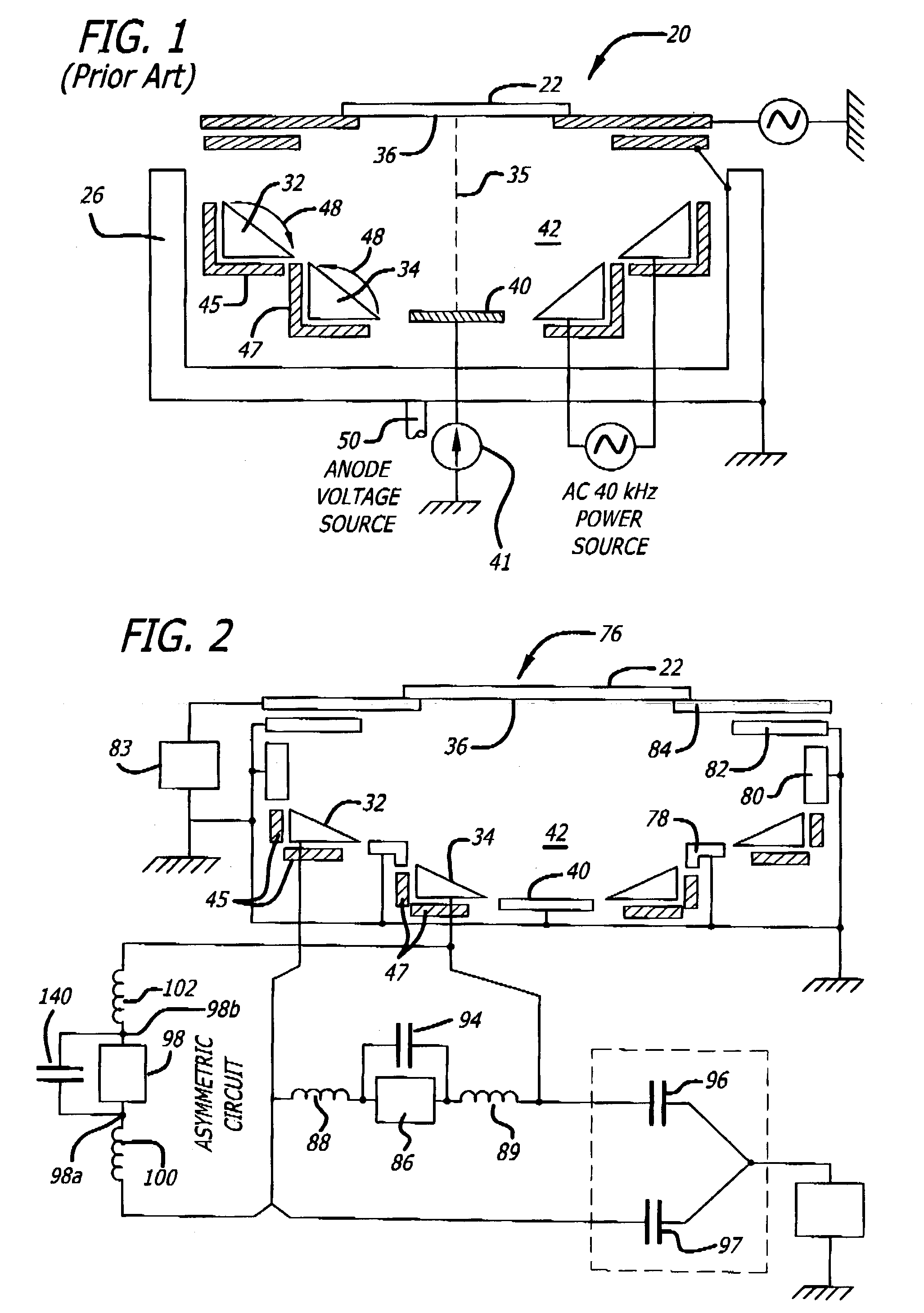
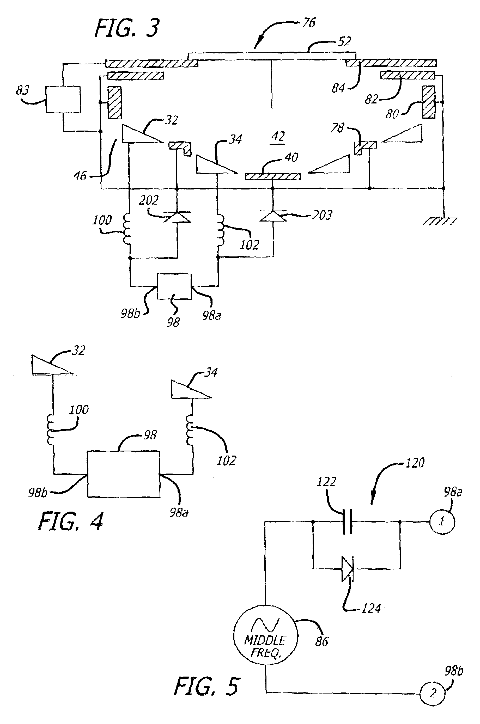
[0011]A system applies an asymmetric alternating voltage (preferably 40 KHz) modulated by RF (e.g. 13.56 MHz) power between a pair of targets having a coaxial relationship and uses an additional diode circuit in order to:

[0012]1. Eliminate dielectric material from the surfaces of the targets during the deposition process and eliminate arcing previously resulting from the deposition of this dielectric material on the target surfaces;

[0013]2. Provide a uniform coating by adjusting the level of asymmetry (applying different levels of power to the individual ones of the targets);

[0014]3. Provide a smooth ignition of the targets due to permanent ionization of the target vicinity resulting from RF discharge.

[0015]4. Reduce defects and foreign particles in the deposited film by eliminating any voltage spike during the target ignition.

[0016]5. Reduce the temperature of the substrate by preventing low energy (“cold”) electrons from the plasma discharge from reaching the substrate;

[0017]6. Pr...


PUM

PropertyMeasurementUnit
frequencyaaaaaaaaaa
frequencyaaaaaaaaaa
frequencyaaaaaaaaaa

Abstract

An asymmetric alternating voltage (preferably 40 KHz) is provided between a pair of targets having a coaxial (preferably frusto-conical) relationship to (1) deposit the material in a uniform thickness on the substrate surface (2) eliminate dielectric material from the surfaces of the targets and other components (3) provide a single ignition of the targets and eliminate target ignitions thereafter and (4) reduce the substrate temperature by using low energy (“cold”) electrons from a plasma discharge to produce a low energy current. The asymmetry may result from amplitude differences between the voltage in alternate half cycles and the voltage in the other half cycles. A second alternating voltage (preferably radio frequency) modulates the asymmetric alternating voltage to provide the smooth plasma ignition. The different voltage amplitudes applied to each of the targets are also instrumental in providing for a substantially constant deposition thickness at the different positions on the surface of the substrate.

Description

[0001]This application is a non-provisional application corresponding to a provisional application filed in the United States Patent and Trademark Office on or about Dec. 12, 2002 and entitled REACTIVE SPUTTERING OF SILICONE NITRIDE FILMS BY RF SUPPORTED DEC MAGNETRON and listing Pavel N. Laptev and Valery V. Felmetsger as joint inventors.[0002]This invention relates to a system for, and method of, producing a deposition of material on a substrate. More particularly, the invention relates to a system for, and method of, producing on a substrate a deposition that provides a uniform coating.BACKGROUND OF THE INVENTION[0003]Integrated circuit chips are being used now in all kinds of apparatus to provide complex electrical circuitry for controlling different operations or for providing data and mathematical calculations in business, education, science and many other fields. With progressive advances in time, the size of the integrated circuit chips has progressively decreased. Even as t...

Claims


Application Information

Patent Timeline
Patent Type & Authority Patents(United States)
IPC IPC(8): C23C14/34C23C14/35H01J37/34
CPCC23C14/352H01J37/3444H01J37/3405H01J37/34
Inventor LAPTEV, PAVEL N.FELMETSGER, VALERY V.
Owner OEM GRP LLC
Why Eureka
Try Eureka