High-speed level sensitive scan design test scheme with pipelined test clocks

a technology of scan design and test scheme, applied in the field of design automation, can solve the problems of increasing the difficulty of distributing shift a and shift b clocks at very high frequencies, affecting the design of complex combinatorial and sequential logic circuits, and increasing the cost of fault-oriented approaches

Inactive Publication Date: 2007-02-13
INT BUSINESS MASCH CORP
View PDF7 Cites 6 Cited by
  • Summary
  • Abstract
  • Description
  • Claims
  • Application Information

AI Technical Summary

Benefits of technology

[0019]Accordingly, it is an object of the invention to provide a method for allowing higher test clock frequencies by combining LSSD testing techniques with a clock tree latency configuration.
[0020]It is another object to provide a method for achieving higher functional performance based on an improved test clock frequency.
[0021]It is still another object to improve testing throughput by reducing testing time, resulting in significant savings in expensive testing hardware.
[0023]It is a yet a further object to provide an apparatus that enhances the distribution of the Shift A and Shift B clock signals to points throughout the entire chip, with a distribution network that is tailored according to a desired LBIST speed.
[0024]The invention provides a method for improving the frequency of test clocks in a Level Sensitive Scan Design (LSSD) system wherein non-overlapping Shift A and Shift B test clocks are synchronized to rise and fall simultaneously at inputs of all LSSD registers, the method includes the steps of: a) determining the number of pipeline stages needed to reach the farthest corner of the system to establish the depth of the pipeline; b) grouping the LSSD registers into regions defined by the number of pipeline stages needed to ensure high speed operation; c) balancing the pipeline depth to achieve a simultaneous rise or fall of a signal at the inputs of the LSSD registers; and d) ensuring that all test clocks are distributed at high speed, and verifying that all the pipeline latches are placed in a predetermined proximity to the LSSD registers to enable high speed synchronous propagation of the Shift A and Shift B test clocks.
[0025]The pipeline latches mentioned above are clocked from the system clock, and by following the series of steps described, the Shift A and Shift B test clocks are guaranteed to be synchronized with the system clock across the entire system. Further, the approach of using latches to pipeline and synchronize the test clocks eliminates the uncertainties usually associated with the distribution of such clocks to every LSSD register in a complicated VLSI design. In this way, the Shift A and Shift B clocks can be reliably designed to run at much higher frequencies than would otherwise be practical using conventional techniques.

Problems solved by technology

In view of the foregoing, it appears that the best stuck fault test algorithms are only computationally feasible for fairly small or fairly simple networks and fault-oriented approaches become prohibitively expensive with the increasing circuit density of VLSI chips and modules.
There are several issues and problems when designing LSSD systems.
Given that actual chips have hundreds of thousands of LSSD latches, one may expect to encounter extremely complicated routing and buffering trees for the Shift A and Shift B clock signals.
Now, as microprocessor (and ASIC chip) frequencies continue to increase, technology scaling provides ever higher circuit densities and chips continue to increase in size, it is becoming increasingly difficult to distribute the Shift A and Shift B clocks at very high frequencies, given the design constraints described previously.
However, it is apparent that this technique leads to a proliferation in the number of latches needed to design the chip.
Since the test clocks have to be distributed to each latch, increasing the number and density of latches on the chip in the manner described above leads to an increase in the complexity of the test clock distribution, causing the overall propagation time (and associated timing uncertainties) to increase as well.
These requirements effectively limit the frequency of the test clocks.
In addition, as the chip frequency increase when segmenting the logic into ever finer slices, it is apparent that this segmentation will not help to speed up the distribution of the test clocks (it actually hinders it, as described above, since the number of latches increases).
Thus, the imbalance between the microprocessor frequency and test clock frequency tends to increase when this technique is utilized.
It is observed that the propagation delay through the test clock network tends to be magnified as a result of these scaling principles, and the larger uncertainties associated with these larger delays again limits the frequency of the test clocks.
Thus, in addition to the two factors described above, the increase in the number and density of latches on the chip greatly increases the difficulty of the test clock distribution problem.
This extra delay leads to an additional uncertainty and disparity in the clock arrival times at the latches, which again will have a negative impact on the maximum test clock frequency.
Accordingly, the conventional scan clock test methodology of this type is not ideal in various ways.
First, LBIST time is relatively long because the rate at which data is scanned through all the LSSD registers is limited by the slow test clocks.
Second, since scanning occurs at a low frequency, power is relatively low during scanning, but the chip will see large power transients when the functional clocks are fired during LBIST testing.
Third, the overall timing relationships between the Shift A and Shift B clock distributions and the functional clock, and the test control signal distribution are unknown and vary across the chip.
This gap further exacerbates power transients during test, and limits the testability or test strategy in certain ways.
Finally, since Shift A and Shift B clocks run at different frequencies from the functional clocks, a separate timing verification process is usually needed, and possibly even a separate set of timing models needs to be generated, all of which requires considerable additional work for the design team.
This technique solves the problems mentioned above, but introduces new issues of its own.
First, there is no capability for driving separate test clocks into the chip from external inputs (since there is no separate test clock any longer).
This increases the delay and / or the power consumption, and possibly the area.
Furthermore, if any of the control signals is slower than expected or slower than the particular logic or does not meet the full frequency timing requirement anywhere in its distribution network, the frequency at which the chip is to be tested will be limited.

Method used


Image

  • High-speed level sensitive scan design test scheme with pipelined test clocks
  • High-speed level sensitive scan design test scheme with pipelined test clocks
  • High-speed level sensitive scan design test scheme with pipelined test clocks

Examples


Embodiment Construction

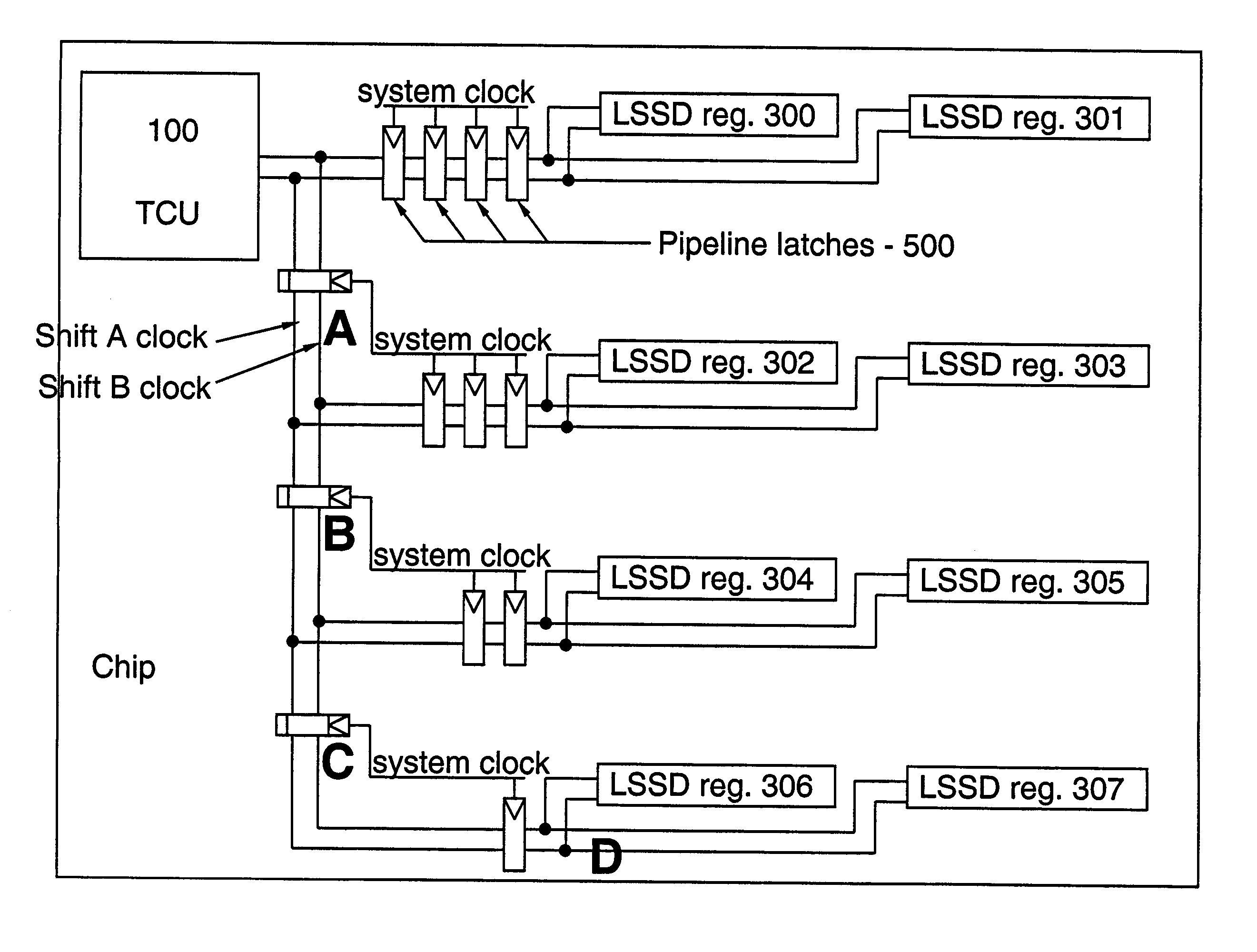
[0033]The inventive method is designed to enhance a standard LSSD configuration by way of small pipeline latches (clocked off the system, functional clock) to distribute the Shift A and Shift B clock signals to various points throughout a VLSI design, with a distribution network that is tailored according to the desired Shift A and Shift B clock frequencies. Using the pipeline latches for distribution of the Shift A and Shift B clocks allows the clock edges to be synchronized across the entire system, but still allows control of the Shift A and Shift B clock periods (with a granularity now measured in units of system clock cycles) in an arbitrary fashion. Using this type of architecture, LBIST is preferably designed to run at frequencies of up to one-half the system clock frequency (compared to one-sixteenth for a more typical LSSD scheme). Also, since the main portion of the Shift A and Shift B clock distributions are through pipeline latches, the arrival times of the Shift A and S...


PUM


Abstract

This invention describes a method of synchronizing test clocks in an LSSD system to achieve near simultaneous arrival of the clock signals at the inputs of all LSSD registers. The method relies on pipelining the latches to distribute the test clocks, where all pipeline latches are synchronized by the system clock. This enhancement improves the frequency at which the test clocks switch and improve the testing throughput by reducing testing time, resulting in significant reductions in testing hardware and overall time required for system test, without compromising any of the benefits associated with conventional LSSD techniques. The method further enhances the distribution of the test clock signals to points throughout the entire chip, with a distribution network that is tailored according to a desired LBIST speed.

Description

BACKGROUND OF THE INVENTION[0001]The present invention relates, generally, to the field of Design Automation, and more specifically, to the design of complex combinatorial and sequential logic circuits embodied in very large scale integration (VLSI) circuit devices.[0002]Faults occurring anywhere in VLSI circuit devices can have their effect propagated through a number of feedback loops formed of storage or memory elements in the sequential logic before reaching a test-able output of the device. Level Sensitive Scan Design (LSSD) rules were devised to eliminate complications in testing caused by this propagation through the feedback loops. As described by E. B. Eichelberger and T. W. Williams in an article entitled “A Logic Design Structure for LSI Testability” on pages 462–468 of the Proceedings of the 14th Design Automation Conf. LSSD rules impose a clocked structure on the memory elements of logic circuits and require that these memory elements be interconnected to form a shift r...

Claims


Application Information

Patent Timeline
Patent Type & Authority Patents(United States)
IPC IPC(8): G01R31/28
CPCG01R31/318594
Inventor WARNOCK, JAMES D.HUOTT, WILLIAM V.
Owner INT BUSINESS MASCH CORP
Why Eureka
Try Eureka