
Communication mechanism

a communication mechanism and semiconductor technology, applied in the field of semiconductor integrated circuits, can solve the problems of increasing the number of wires, increasing delay, becoming impractical, etc., and achieve the effects of facilitating wire distribution around the chip, facilitating wire placement and routing, and increasing the distance of wires

Active Publication Date: 2006-12-26
CALLAHAN CELLULAR L L C
View PDF5 Cites 10 Cited by
  • Summary
  • Abstract
  • Description
  • Claims
  • Application Information

AI Technical Summary

Benefits of technology

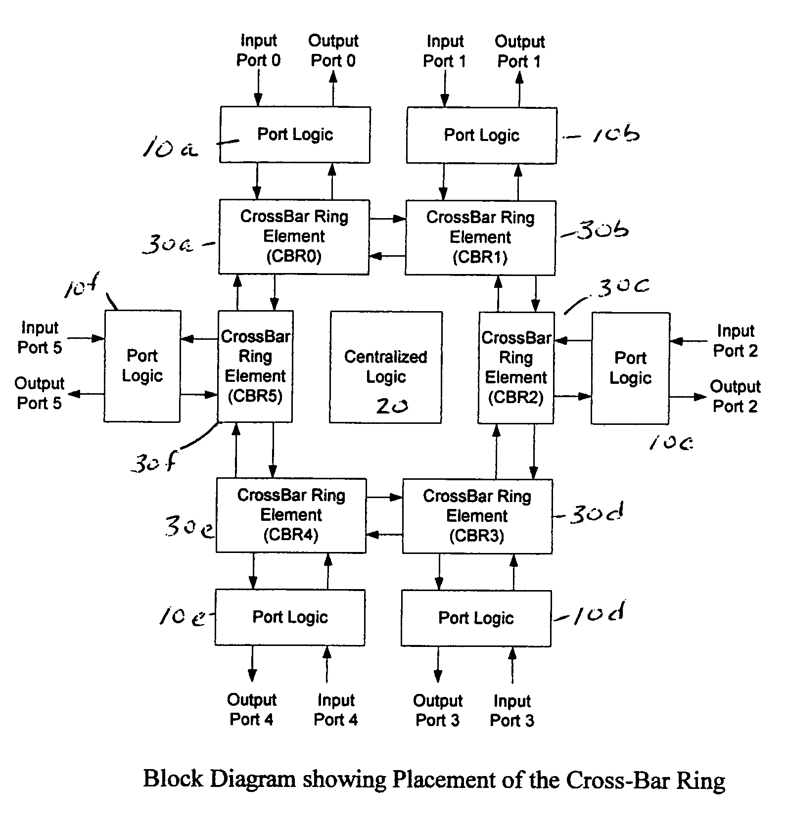
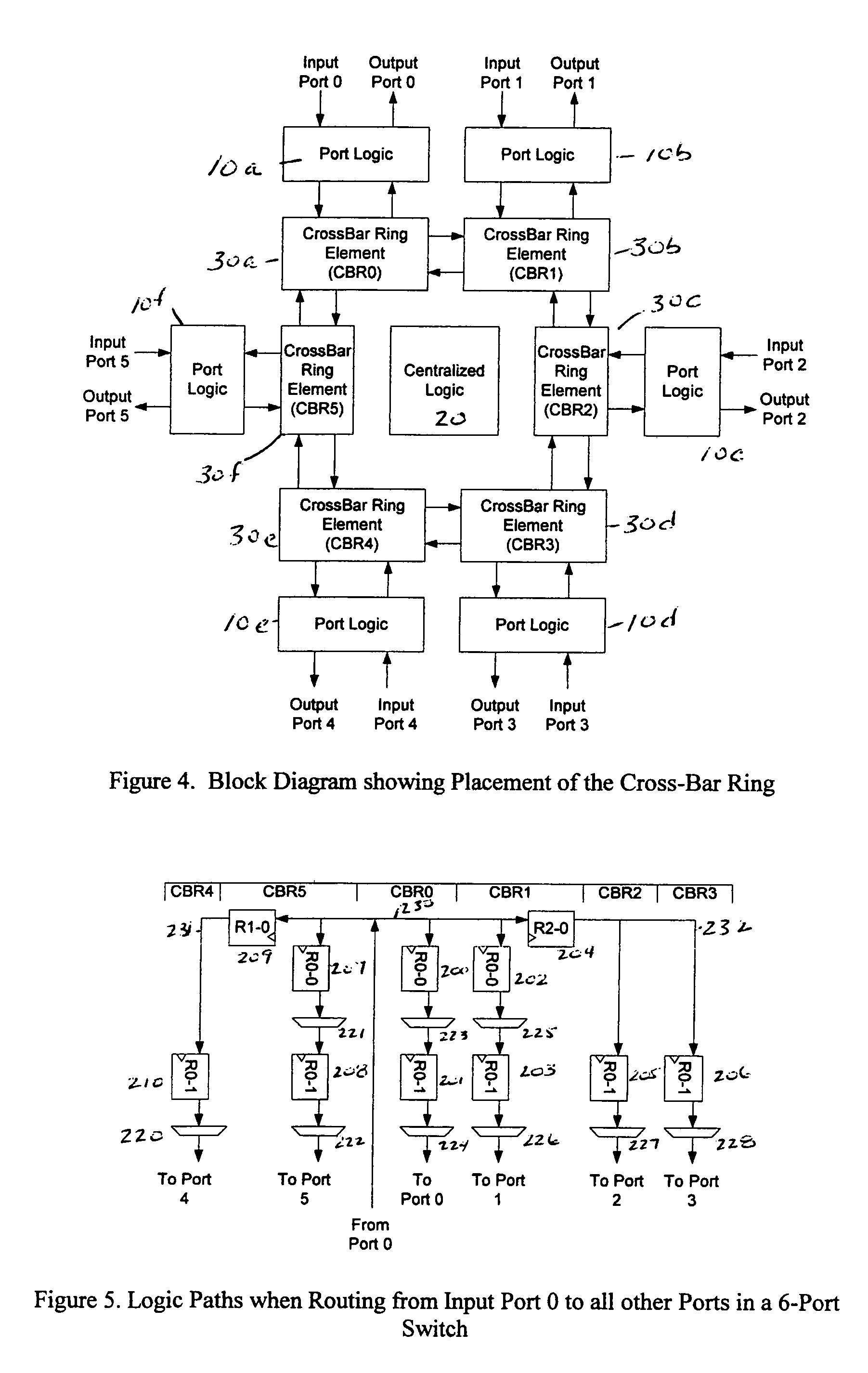
[0008]The problems with the prior art have been overcome with this invention, which provides an interconnection architecture for semiconductor devices. Cross bar switches are traditionally placed in the center of the IC. However, this location may also be the preferred location for the centralized logic in the IC. This invention, known as a cross bar ring or CBR, provides cross bar switch functionality in a manner that can be easily distributed around the chip. Typically, it can fit in the routing channels between other functional blocks, thereby allowing other centralized functions to be placed in the center of the IC. The CBR is defined so that it can be partitioned into separate modules, which greatly aids in the placement and routing of wires. Furthermore, the architecture is defined such that the CBR can use storage elements, allowing it to be pipelined so that the wire distances can be increased while still maintaining a high internal clock speed. The use of storage elements also allows the CBR to provide a deterministic delay between any two locations on the IC, and can, if desired, insure a constant delay regardless of source and destination.

Problems solved by technology

However, as the value of N increases, the number of wires increases exponentially, thereby becoming impractical.
Large numbers of connections create complications within the IC, as there is only a limited amount of space within the IC that can be used for routing wires.
Therefore, if a connection is not a straight line, it will have to use valuable space on multiple routing layers to achieve the required connection.
A second complication in the routing of wires within a IC device is timing.
Therefore, as wires get longer, the delay also increases and it takes a greater amount of time for a signal to propagate from one end of the wire to the other end.
In fact, when an IC is being developed, it is common that the propagation delay of certain wires can exceed the clock cycle.
In extreme cases, the wire, and the delay, cannot be shortened enough.
These changes can force schedule delays, which are obviously undesirable.
This can be problematic if the chip has other centralized functions that would be best located in the center of the IC.

Method used


Image

  • Communication mechanism
  • Communication mechanism
  • Communication mechanism

Examples


Embodiment Construction

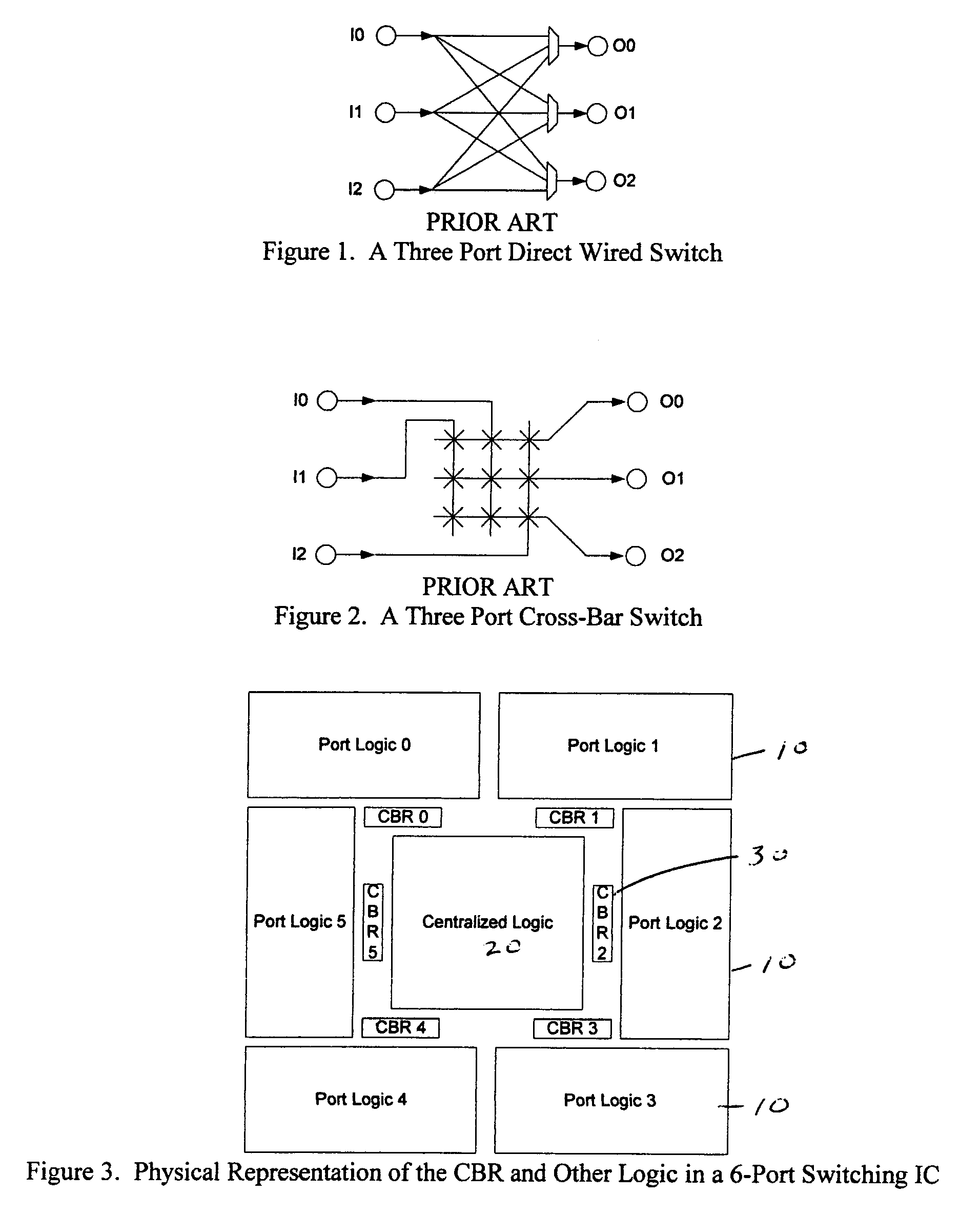
[0017]Switches are used to logically connect a set of input ports to a set of output ports. FIG. 3 shows a typical block diagram of a network switching device. This block diagram is also a physical layout or placement of the functional blocks within the device. Around the outer ring of the chip are 6 functional blocks 10, each associated with a particular input and output port. In the case of many switches, this port logic 10 is identical for each of the ports, although there is no requirement that this be the case. The port logic typically contains functions specifically associated with a particular port, such as transceivers, logic to determine a packet's port and class, FIFOs or buffers for incoming and outgoing packets. Physically located in the center of the IC is the centralized logic 20. Typically, this block 20 contains logic that allows the separate port logic blocks 10 to operate together as a single switch. Functions such as scheduling and centralized buffering, routing t...


PUM


Abstract

The invention provides an interconnection architecture for semiconductor devices. Cross bar switches are traditionally placed in the center of the IC. However, this location may also be the preferred location for the centralized logic in the IC. This invention, known as a cross bar ring or CBR, provides cross bar switch functionality in a manner that can be easily distributed around the chip. Typically, it can fit in the routing channels between other functional blocks, thereby allowing other centralized functions to be placed in the center of the IC. The CBR is defined so that it can be partitioned into separate modules, which greatly aids in the placement and routing of wires. Furthermore, the architecture is defined such that the CBR can use storage elements, allowing it to be pipelined so that the wire distances can be increased while still maintaining a high internal clock speed. The use of storage elements also allows the CBR to provide a deterministic delay between any two locations on the IC, and can, if desired, insure a constant delay regardless of source and destination.

Description

BACKGROUND OF THE INVENTION[0001]In many semiconductor integrated circuit (IC) applications, it is desirable and necessary to pass information between different, physically separate portions of the IC. For example, within a microprocessor IC, address and data paths travel between the various functional blocks, such as adders, register banks and caches. Similarly, data travels between the various ports of a network switching device. In this latter case, it is common that there are multiple sets of data traveling between various portions of the device. For example, the chip may be transmitting data from a first input port to a first output port, while it is simultaneously transmitting data between a second input port and a second output port. Therefore, there is a need to quickly and efficiently allow the movement of data between a plurality of destinations within the IC. A variety of methods have been designed to address this issue. FIG. 1 shows a simple circuit where each input is d...

Claims


Application Information

Patent Timeline
Patent Type & Authority Patents(United States)
IPC IPC(8): G06F13/00
CPCH04L49/102H04L49/101
Inventor MEIER, KARL
Owner CALLAHAN CELLULAR L L C
Learn More