
Process monitoring for ferroelectric memory devices with in-line retention test

a ferroelectric memory and process monitoring technology, applied in the field of memory devices, can solve the problems of affecting the performance of ferroelectric capacitors, requiring personal devices that require more computational power and on-chip memory, so as to facilitate the evaluation of ferroelectric memory devices, avoid unnecessary thermal bake performance, and fast and low cost

Active Publication Date: 2006-12-12
TEXAS INSTR INC
View PDF8 Cites 26 Cited by
  • Summary
  • Abstract
  • Description
  • Claims
  • Application Information

AI Technical Summary

Benefits of technology

The present invention relates to the fabrication and modification of ferroelectric memory devices, which are either stand-alone devices or integrated onto a semiconductor chip that includes other device types. Additionally, the present invention provides a relatively fast and low cost mechanism of identifying data retention lifetimes of ferroelectric memory devices. This mechanism involves obtaining polarization values following a short delay and a long delay after a programming pulse. The short delay is short enough that substantial relaxation has not occurred whereas the long delay is long enough that substantial relaxation has occurred. The differences between the short delay and long delay polarization values are indicators of data retention lifetimes of subject ferroelectric memory devices. This allows for the avoidance of unnecessary performance of thermal bake data retention lifetime testing. The invention also includes the features of fabricating and modifying ferroelectric memory devices, as well as characterizing and evaluating fabricated ferroelectric memory devices.

Problems solved by technology

In addition to being smaller and more portable, personal devices are requiring more computational power and on-chip memory.
A characteristic of the shown ferroelectric memory cell is that a read operation is destructive.
However, over time, the ferroelectric properties of the ferroelectric capacitor can alter.
However, over time, the bi-stable characteristic can degrade significantly and negatively affect data retention.
Thus, ferroelectric memory devices can, over time, become unusable for some applications.
However, conventional testing mechanisms can be costly, time consuming, and destructive to the ferroelectric cells being tested.
The baking of memory arrays and / or devices as part of a test flow can potentially reduce the lifetime of the part, therefore, screening methods that include a thermal bake can also compromise the reliability of the memory device, even if the wares are not totally destroyed.
Furthermore, conventional testing mechanisms can destroy the wafer upon which the devices are formed, thereby mitigating use on large numbers of wafers and / or devices.

Method used


Image

  • Process monitoring for ferroelectric memory devices with in-line retention test
  • Process monitoring for ferroelectric memory devices with in-line retention test
  • Process monitoring for ferroelectric memory devices with in-line retention test

Examples


Embodiment Construction

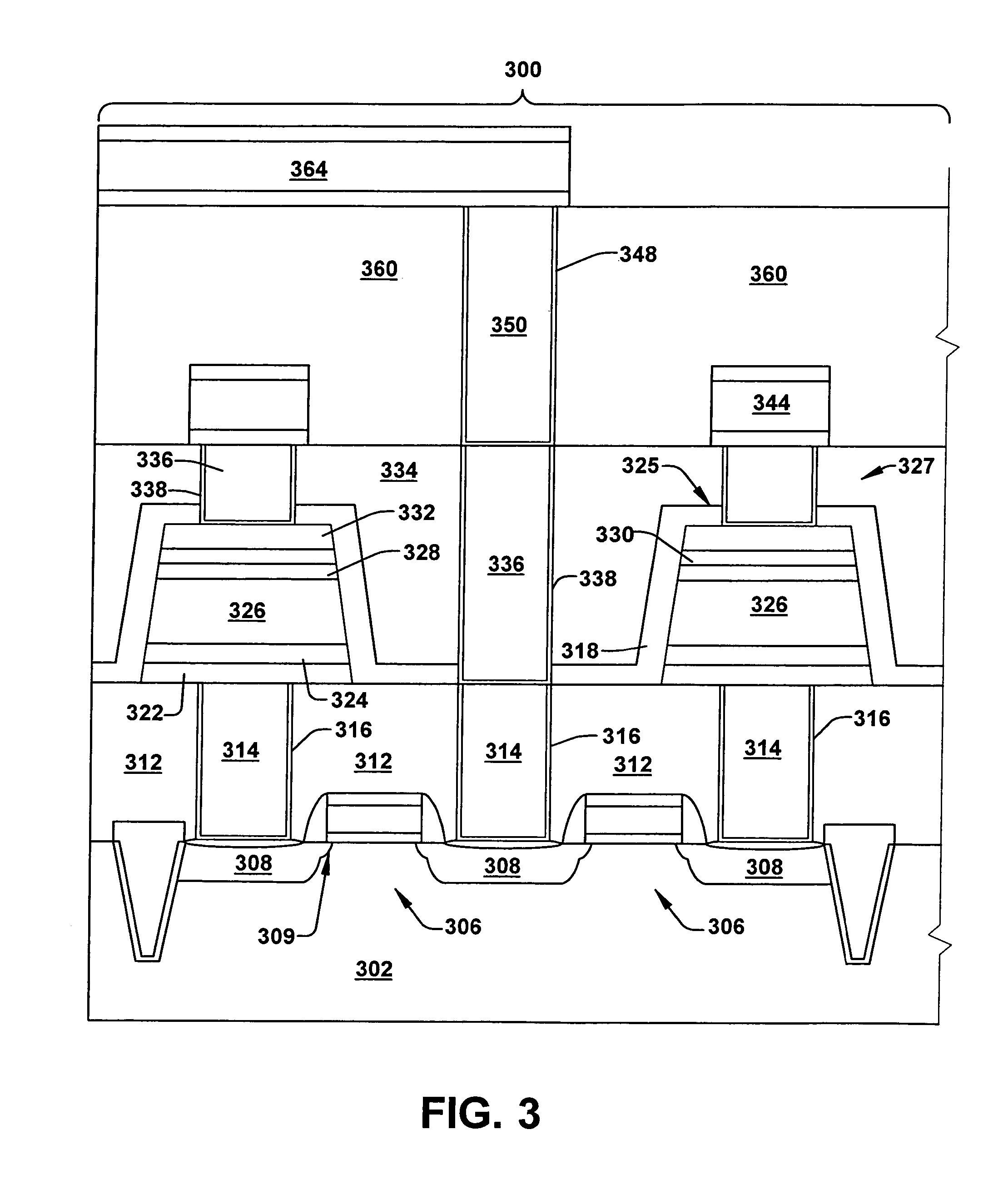
[0033]The present invention will now be described with respect to the accompanying drawings in which like numbered elements represent like parts. The figures provided herewith and the accompanying description of the figures are merely provided for illustrative purposes. One of ordinary skill in the art should realize, based on the instant description, other implementations and methods for fabricating the devices and structures illustrated in the figures and in the following description.

[0034]The present invention relates to the evaluation and characterization of ferroelectric memory devices after fabrication. The present invention can identify data retention limitations and other ferroelectric device fabrication problems without extensive testing. The present invention facilitates evaluation of ferroelectric memory devices by providing a relatively fast and low cost mechanism of identifying data retention lifetimes. The mechanism obtains short delay and long delay polarization value...


PUM


Abstract

The present invention facilitates evaluation of ferroelectric memory devices. A ferroelectric memory device is fabricated that comprises memory cells comprising ferroelectric capacitors (802). A short delay polarization value is obtained (804) by writing a data value, performing a short delay, and reading the data value. A long delay polarization value is obtained (806) by again writing the data value, performing a long delay, and again reading the data value. The short delay and long delay polarization values are compared (808) to obtain a data retention lifetime for the ferroelectric memory device. The obtained data retention lifetime is compared with acceptable values (810) and, if deemed unacceptable, avoids unnecessary performance of thermal bake data retention lifetime testing.

Description

FIELD OF THE INVENTION[0001]The present invention relates generally to memory devices, and more particularly, to systems and methods that evaluate operation and retention reliability of ferroelectric memory devices.BACKGROUND OF THE INVENTION[0002]Several trends exist today in the semiconductor device fabrication industry and the electronics industry. Devices are continuously getting smaller and requiring less power. A reason for this is that more personal devices are being fabricated that are relatively small and portable, thereby relying on a small battery as its supply source. For example, cellular phones, personal computing devices, and personal sound systems, personal digital assistants, and the like are devices that are in great demand in the consumer market. In addition to being smaller and more portable, personal devices are requiring more computational power and on-chip memory. In light of these trends and others, there is a need in the industry to provide devices that have...

Claims


Application Information

Patent Timeline
Patent Type & Authority Patents(United States)
IPC IPC(8): G11C7/00
CPCG11C11/22G11C29/50G11C29/50016
Inventor RODRIGUEZ, JOHN ANTHONYBAILEY, RICHARD ALLEN
Owner TEXAS INSTR INC
Learn More