
CAD method for arranging via-holes, a CAD tool, photomasks produced by the CAD method, a semiconductor integrated circuit manufactured with photomasks and a computer program product for executing the CAD method

a cad method and via-hole technology, applied in the field of computer-aided design (cad) methods, can solve the problems of defective connection generation, wiring failure such as disconnection, and difficulty in establishing the geometry of metallic wiring configured to interconnect circuit elements as designed

Active Publication Date: 2006-12-05
KK TOSHIBA
View PDF9 Cites 5 Cited by
  • Summary
  • Abstract
  • Description
  • Claims
  • Application Information

AI Technical Summary

Problems solved by technology

Recently, with the miniaturization of the feature size of semiconductor integrated circuits, it becomes difficult to establish a geometry of metallic wirings configured to interconnect between circuit elements as designed.
And because of misalignment in overlay accuracy from upper to lower wiring levels, in the photolithography process, such a phenomenon (shortening) occurs, as an upper metallic wiring does not reach the position of a via-hole which is supposed to connect the upper metallic wiring to a lower metallic wiring, and defective connection is generated.
And, with advancements in miniaturization of semiconductor integrated circuits, since it becomes difficult to bury metallic material in a small via-hole, wiring failures such as disconnection and poor contact occur.
However, according to the above-mentioned CAD method, where a wiring grid (wiring lattice) is first set at each wiring level and metallic wirings are arranged in reference to the wiring grid, wiring efficiency becomes low because the extension regions occupy the triple wiring lattices (the wiring grid) located adjacent both sides of the corresponding metallic wiring.
Especially, in a case where more than two via plugs were formed in the termination of metallic wiring, extension regions in a large area spanning over more than two via plugs must be established, and the extension regions an even larger space to include additional wiring grids located adjacent on both sides of the corresponding metallic wiring, this causes even lowered wiring efficiency.

Method used


Image

  • CAD method for arranging via-holes, a CAD tool, photomasks produced by the CAD method, a semiconductor integrated circuit manufactured with photomasks and a computer program product for executing the CAD method
  • CAD method for arranging via-holes, a CAD tool, photomasks produced by the CAD method, a semiconductor integrated circuit manufactured with photomasks and a computer program product for executing the CAD method
  • CAD method for arranging via-holes, a CAD tool, photomasks produced by the CAD method, a semiconductor integrated circuit manufactured with photomasks and a computer program product for executing the CAD method

Examples


first embodiment

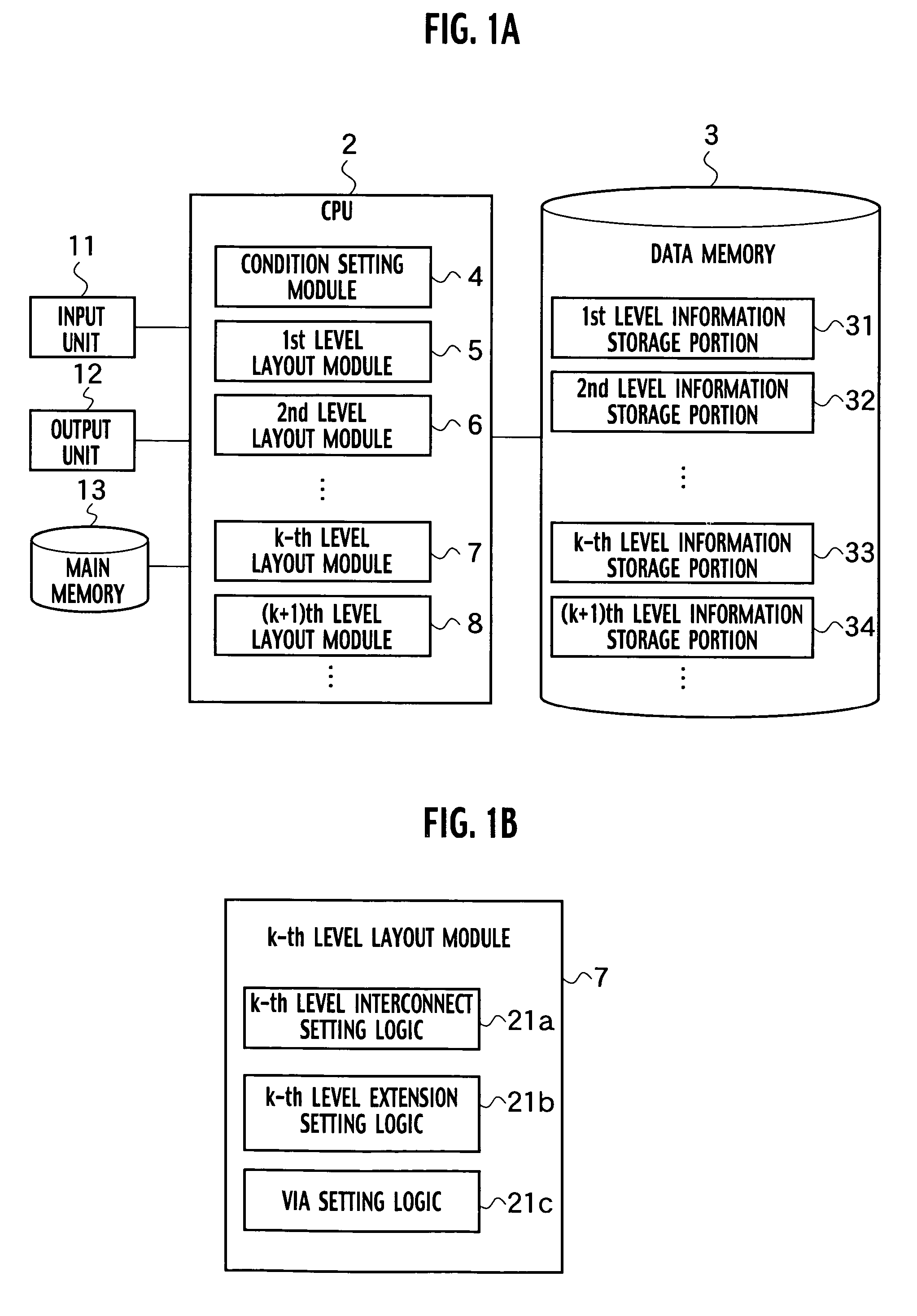
[0053]As shown in FIG. 1A, a designing tool according to a first embodiment of the present invention includes a central processing unit (CPU) 2, a data memory 3, an input unit 11, an output unit 12 and a main memory 13.

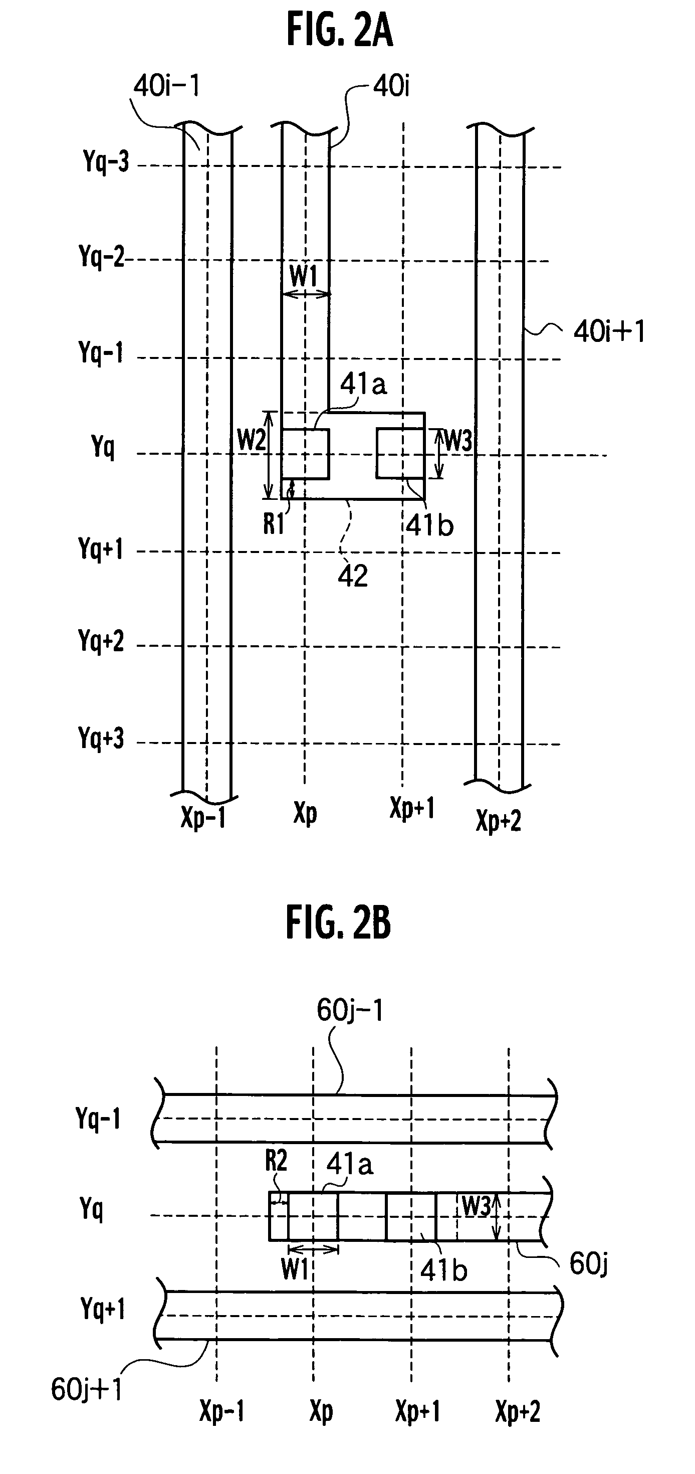
[0054]As shown in FIG. 2A and FIG. 2B, the CPU 2 executes the processing of the designing tool on the basis of wiring grids which are implemented by a plurality of regularly spaced first lines Xp−1, Xp, Xp+1, . . . , each of which runs in parallel along a fixed direction (vertical direction) and by a plurality of regularly spaced second lines Yq−1, Yq, Yq+1, . . . , each of which runs in parallel along such a direction (horizontal direction) as intersects orthogonally to the regularly spaced first lines Xp−1, Xp, Xp+1, . . . (“p” and “q” are integers, respectively). Therefore, the CPU 2 encompasses a condition setting module 4 configured to set the wiring condition of specific wiring level, a first level layout module 5 configured to layout the first wiring level, a s...

second embodiment

[0133]As already shown in the common block diagram of FIG. 1A, a designing tool according to a second embodiment of the present invention includes a central processing unit (CPU) 2, a data memory 3, an input unit 11, an output unit 12 and a main memory 13. Herein, only features different from the designing tool according to the first embodiment are mainly described, while the features which are equivalent to those appearing in the first embodiment, are omitted since they are substantially similar.

[0134]As shown in FIG. 10A, the k-th level interconnect setting logic 21a shown in FIG. 1B, designs layouts of a first strip pattern 240i−1 of the k-th wiring level, a second strip pattern 240i of the k-th wiring level and a third strip pattern 240i+1 the k-th wiring level which extend in the k-th wiring level along the k-th level priority direction.

[0135]The k-th level extension setting logic 21b generates a pattern of a k-th level extension 242 extending in a direction intersecting slanti...

third embodiment

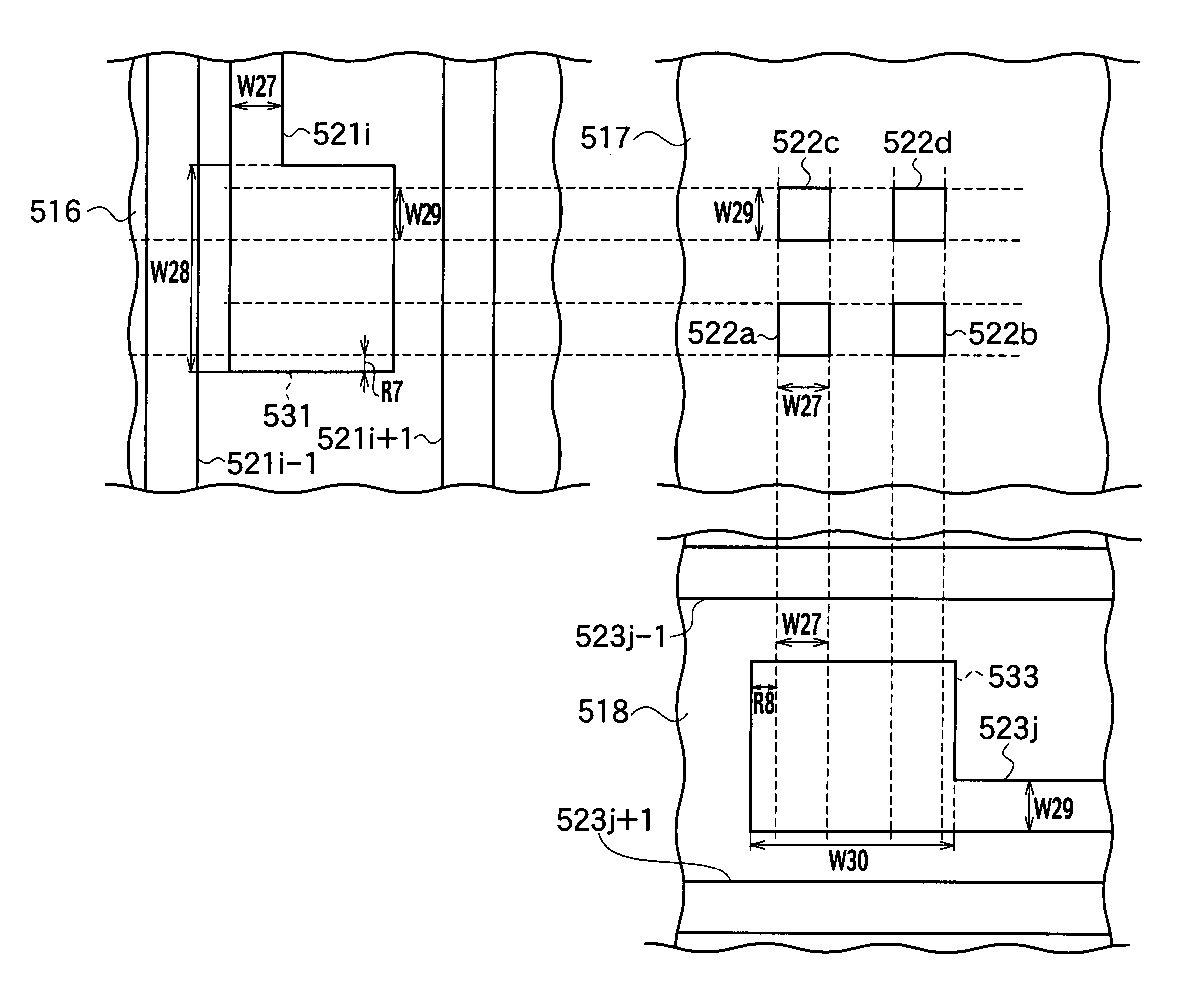
[0176]As already shown in the common block diagram of FIG. 1A, a designing tool according to a third embodiment of the present invention includes a central processing unit (CPU) 2, a data memory 3, an input unit 11, an output unit 12 and a main memory 13. Herein, only features different from the designing tool according to the first embodiment, are mainly described, while the features which are overlapped with the first embodiment are omitted since they are substantially similar.

[0177]As shown in FIG. 13A, the k-th level interconnect setting logic 21a shown in FIG. 1B, designs layouts of a first strip pattern 440i−1 of the k-th wiring level, a second strip pattern 440i of the k-th wiring level and a third strip pattern 440i+1 of the k-th wiring level which extend in the k-th wiring level along the k-th level priority direction.

[0178]The k-th level extension setting logic 21b generates a pattern of a k-th level extension 442 extending in an orthogonal direction to the k-th level prio...


PUM

PropertyMeasurementUnit
thicknessaaaaaaaaaa
thicknessaaaaaaaaaa
widthaaaaaaaaaa

Abstract

A design method encompasses: determining a direction of a subject wiring level in a multi-level interconnection of semiconductor integrated circuit as a subject-level priority direction; designing a layout of the subject wiring level, by placing a subject-level strip extending along the subject-level priority; generating a subject-level extension extending in a different direction of the subject-level priority direction, from a termination of the subject-level strip; allocating via-holes in the subject-level extension; and designing a layout of a neighboring wiring level of the subject wiring level, by placing a neighboring-level strip extending along the same direction as the subject-level extension extends, so that a termination of the neighboring-level strip can include the via-holes.

Description

CROSS REFERENCE TO RELATED APPLICATIONS[0001]This application claims benefit of priority under 35 USC 119 based on Japanese Patent Application No. P2003-343302 filed Oct. 1, 2003, the entire contents of which are incorporated by reference herein.BACKGROUND OF THE INVENTION[0002]1. Field of the Invention[0003]The present invention relates to a computer-aided design (CAD) method, a CAD tool, a set of photomasks produced by the CAD method, a semiconductor integrated circuit manufactured employing the set of photomasks and a computer program product for executing the CAD method, and in particular to a configuration for arranging via-holes at a termination of a interconnection, which implements a multi-level interconnection.[0004]2. Description of the Related Art[0005]Recently, with the miniaturization of the feature size of semiconductor integrated circuits, it becomes difficult to establish a geometry of metallic wirings configured to interconnect between circuit elements as designed. ...

Claims


Application Information

Patent Timeline
Patent Type & Authority Patents(United States)
IPC IPC(8): G06F17/50H01L21/4763H01L23/52G03F1/68G03F1/70G06F9/455H01L21/3205H01L21/768H01L21/82H01L21/822H01L23/522H01L27/04
CPCG03F1/14G06F17/5077G03F1/00G06F30/394
Inventor OTA, YUZO
Owner KK TOSHIBA
Learn More