
Method for measuring impurity metal concentration

a technology of impurity metal and concentration, which is applied in the direction of instrumentation, semiconductor/solid-state device testing/measurement, nuclear elements, etc., can solve the problems of longer elapsed time and longer period of tim

Active Publication Date: 2006-11-28
SUMCO TECHXIV
View PDF9 Cites 15 Cited by
  • Summary
  • Abstract
  • Description
  • Claims
  • Application Information

AI Technical Summary

Benefits of technology

"The present invention provides a method for measuring the metal impurity concentration in a silicon wafer using a surface photovoltage (SPV) method. The method takes into account factors such as the electric resistivity, the period of elapsing time from the activation to the measurement, and the temperature of the silicon wafer. By measuring the minority carrier diffusion length prior to the calibration activation and calculating the metal impurity concentration based on the dependence of the minority carrier diffusion length on at least one factor, the method can account for variations in the factors and obtain accurate measurements. The method can be used to measure the metal impurity concentration in a slicion wafer."

Problems solved by technology

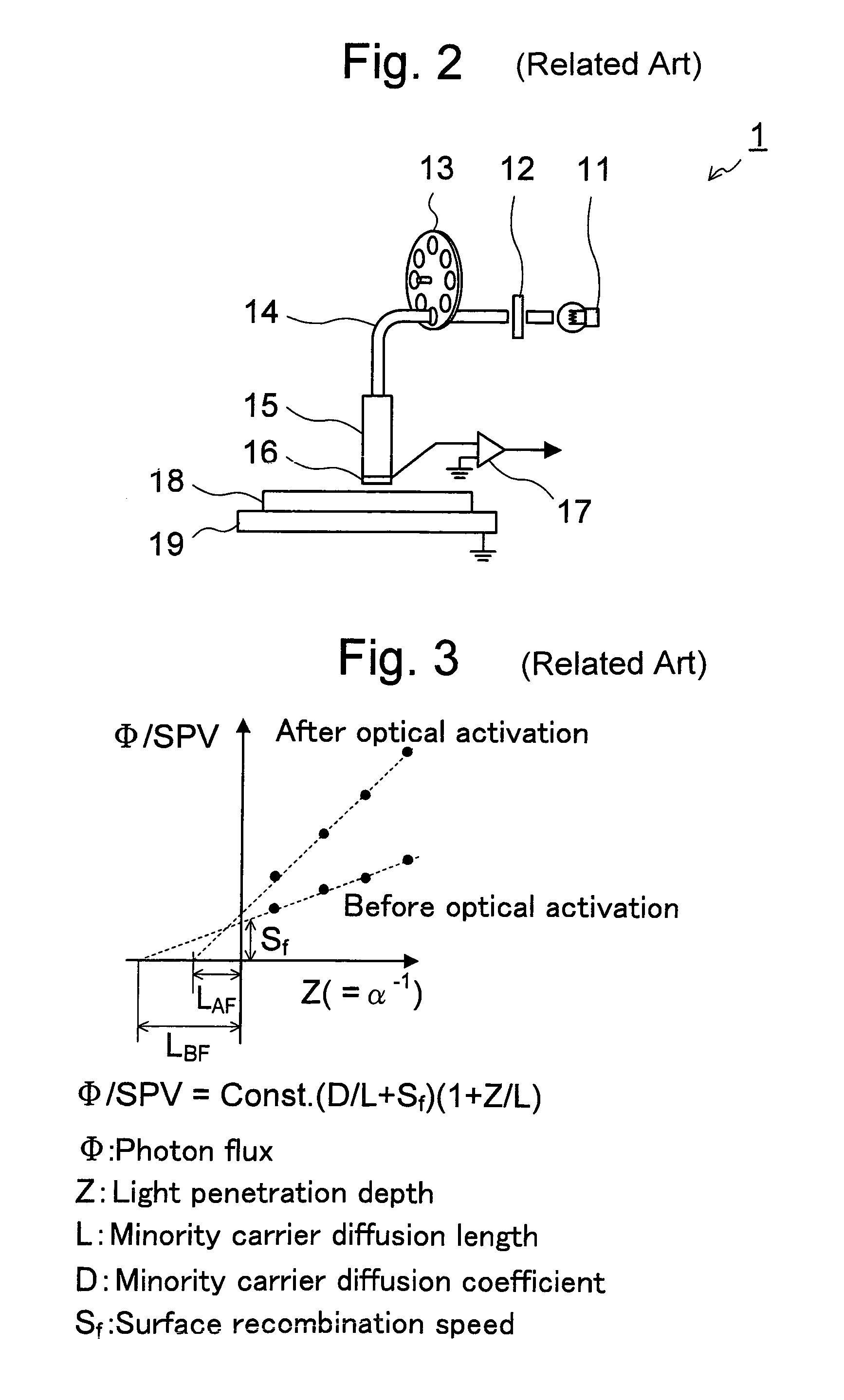
However, a longer period of time may elapse between the activation and the measurement of the minority carrier diffusion length at a more peripheral measuring point if a measuring device having a design (structure) to measure the minority carrier diffusion lengths in the order from the center to the periphery of the silicon wafer as described in the above example when many measuring points are measured by the SPV method.
However, in the silicon wafer having a large diameter (e.g., being equal or larger than 300 [mm]) and a low electric resistivity (e.g., not exceeding 10 [Ω·cm]), it is expected that a larger number of measuring points are required so that the elapsing time has to be longer.

Method used


Image

  • Method for measuring impurity metal concentration
  • Method for measuring impurity metal concentration
  • Method for measuring impurity metal concentration

Examples


simulation example 1

[0096]The inventors conducted a simulation to show that the recombination of the interstitial irons with borons may proceed faster as the electric resistivity of the silicon wafer is lower and as the temperature of the silicon wafer is higher. FIG. 9 illustrates actual results of the simulation. For example, in the case of the silicon wafer being kept at 300 K and having the electric resistivity of 11 Ω·cm, LAF / LBF=0.0420 immediately after the activation (t=0.1 min) as opposed to LAF / LBF=0.0487 at t=200.1 min such that the change thereof is small (a changing rate is 16.0%). On the other hand, in the case of the silicon wafer having the electric resistivity of 1 Ω·cm, LAF / LBF=0.1328 immediately after the activation (t=0.1 min) as opposed to LAF / LBF=0.5105 at t=200.1 min such that the change thereof is huge (a changing rate is 284.4%). This shows that the recombination of Fe—B pairs proceeds faster in the silicon wafer having a lower rigistivity. Also, in the case of the silicon wafer...

experiment 1

[Experiment 1]

[0097]The inventors made the measurement of the iron concentration as an experimental example by the SPV method under various conditions with the correction according to the present invention and compared them with the measured values by the DLTS method. FIGS. 10A, 10B, 11A and 11B show the results. A p-type silicon wafer doped with boron as a dopant was used.

[0098]The measurements of the iron concentrations were made at from the light irradiation (optical activation) to the time having elapsed for 60 min with various kinds of specimens having iron concentrations from an order of 1×10¹¹ to an order of 1×10¹⁴. The temperatures of the specimens were from 28.4 Celsius to 29.9 Celsius. As shown in FIGS. 13A and 13B, plots with the conventional correction (by the equation (1)) are lower than the measured values of the iron concentration by the DLTS method while the plots with a correction according to the present invention match well with the measured values of the iron con...


PUM

PropertyMeasurementUnit
band gapaaaaaaaaaa
diameteraaaaaaaaaa
electric resistivityaaaaaaaaaa

Abstract

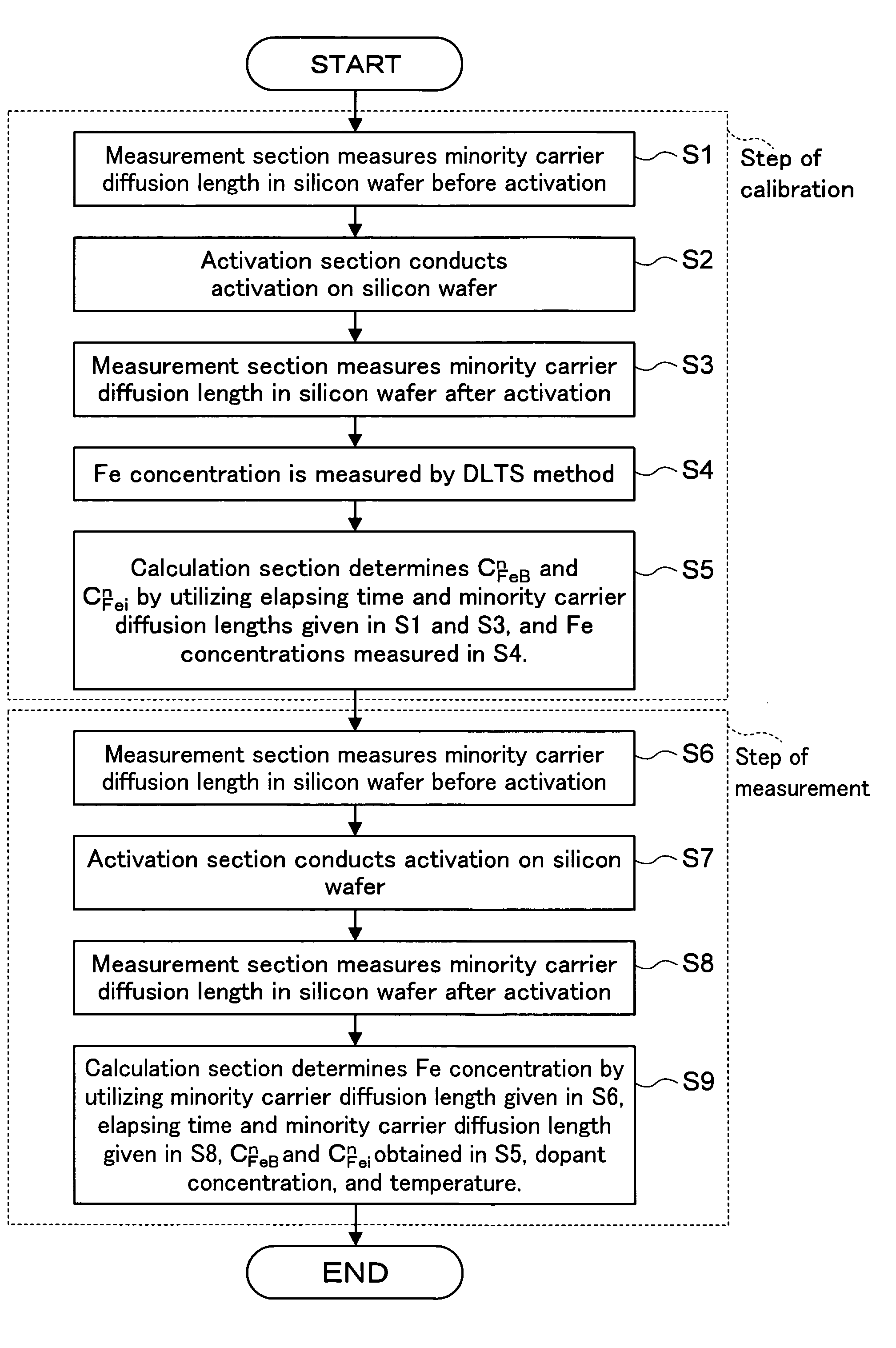
There is provided a method for calculating a more accurate metal impurity concentration contained in a silicon wafer by correcting measured values with a calibration based on a dependent relationship of the minority carrier diffusion length with a period of time elapsing from the activation to the actual measurement, an electric resistivity, and a temperature if there is such a relationship, in the measurement of the metal impurity concentration by utilizing the surface photovoltage. In the calibration step, such dependent relationship may be obtained by utilizing the metal impurity concentration measured by methods of different principles and actually measured values are corrected in light of the dependent relationship in the measuring step such that the metal impurity concentration is measured more accurately.

Description

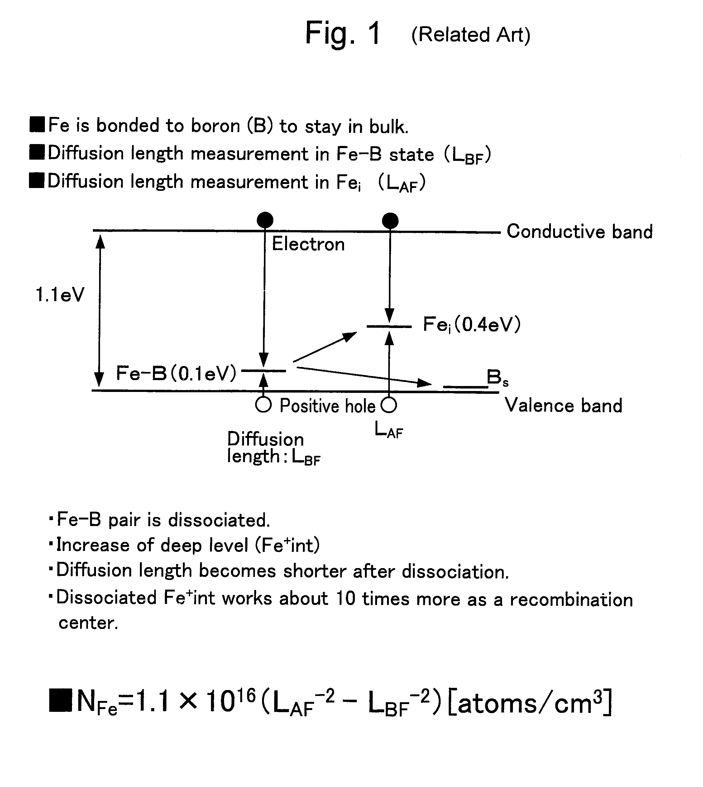
CROSS-REFERENCE TO RELATED APPLICATIONS[0001]This application is based upon and claims the benefit of priority from the prior Japanese Patent Application No. 2004-130234 filed on Apr. 26, 2004, the entire contents of which are incorporated herein by reference.FIELD OF THE INVENTION[0002]The present invention relates to a method for measuring an impurity metal concentration contained in a silicon wafer.RELATED ART[0003]It is understood that it is more preferable to reduce impurity metal contamination in silicon wafers, and it becomes more and more important to reduce such impurity metal contamination as the degree of integration becomes higher. The impurity metal is easily diffused into bulk of silicon wafers by a heat treatment (or thermal annealing) or the like and changes characteristics of the silicon wafers after the thermal annealing. For example, if an iron (Fe) atom diffused into a p-type silicon wafer doped with boron (B) becomes a positive ion, and tends to form a pair with...

Claims


Application Information

Patent Timeline
Patent Type & Authority Patents(United States)
IPC IPC(8): G01R31/302G01R31/26G01R35/00H01L21/66
CPCH01L22/14G01R31/2648G01R35/005
Inventor OHNO, RYUUJIMATSUMOTO, KEI
Owner SUMCO TECHXIV
Learn More