
Method of increasing cell retention capacity of silicon nitride read-only-memory cell

a cell technology, applied in the field of memory fabrication, can solve the problems of lowering the threshold voltage, affecting the performance of the memory, so as to achieve constant threshold voltage and increase the cell retention capacity of the silicon nitride read-only memory cell

Active Publication Date: 2006-11-07
MACRONIX INT CO LTD
View PDF5 Cites 3 Cited by
  • Summary
  • Abstract
  • Description
  • Claims
  • Application Information

AI Technical Summary

Benefits of technology

[0009]Accordingly, one object of the present invention is to provide a method of increasing cell retention capacity of a silicon nitride read-only-memory cell by preventing charges leaking from the charge-trapping layer so that a constant threshold voltage can be maintained.
[0012]Furthermore, with the removal of trapped holes within the tunnel oxide layer of the wafer, hole triggered loss of charges is prevented even if the wafer undergoes a cell retention check thereafter. Ultimately, charge retention capacity of the silicon nitride read-only-memory is effectively increased.

Problems solved by technology

In the process of fabricating the silicon nitride read-only-memory, the two outermost word lines located on each side of the memory cell array are vulnerable to various types of in process damages, ultimately damaging the tunnel oxide layer.
Moreover, some of the steps may require a plasma treatment leading to some holes trapped within the damaged tunnel oxide layer.
If the wafer is damaged so that the tunnel oxide layer contains trapped holes, these holes may induce the charges within the charge-trapping layer to leak into the substrate through the tunnel oxide layer during a cell retention check.
Ultimately, there is a loss of charges leading to a lowering of memory retention capacity and threshold voltage.

Method used


Image

  • Method of increasing cell retention capacity of silicon nitride read-only-memory cell
  • Method of increasing cell retention capacity of silicon nitride read-only-memory cell
  • Method of increasing cell retention capacity of silicon nitride read-only-memory cell

Examples


Embodiment Construction

[0019]Reference will now be made in detail to the present preferred embodiments of the invention, examples of which are illustrated in the accompanying drawings. Wherever possible, the same reference numbers are used in the drawings and the description to refer to the same or like parts.

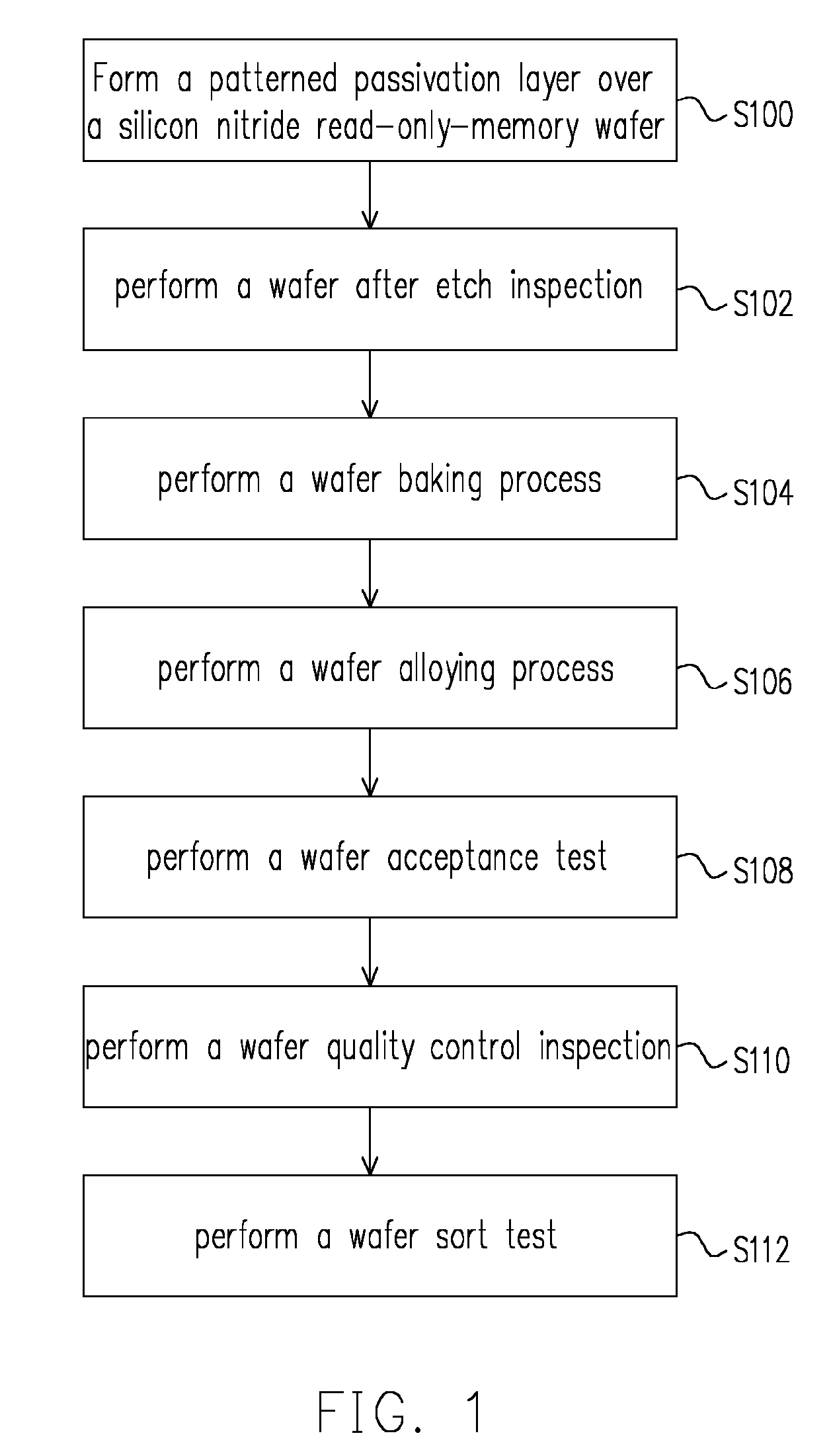
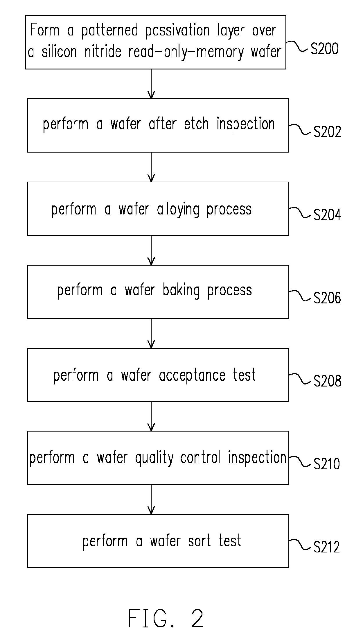
[0020]FIG. 1 is a flow chart showing the steps for increasing cell retention capacity of a silicon nitride read-only-memory cell according to a first preferred embodiment of this invention. In step S100, a patterned passivation layer is formed over a silicon nitride read-only-memory wafer. The steps for forming the patterned passivation layer includes forming a passivation layer over the entire wafer, forming a patterned photoresist layer and removing a portion of the passivation layer using the photoresist layer as an etching mask. Thereafter, the photoresist layer is removed. The step for removing a portion of the passivation layer includes performing a plasma dry etching operation and the step for...


PUM

PropertyMeasurementUnit
temperatureaaaaaaaaaa

Abstract

A method of increasing the cell retention capacity of a silicon nitride read-only-memory on a wafer. The method includes carrying out a baking process after performing the last plasma treatment of the wafer but before a wafer sort test.

Description

CROSS REFERENCE TO RELATED APPLICATIONS[0001]This application claims the priority benefit of Taiwan application serial no. 92117551, filed Jun. 27, 2003.BACKGROUND OF INVENTION[0002]1. Field of Invention[0003]The present invention relates to a method of fabricating memory. More particularly, the present invention relates to a method of increasing the data retention capacity of a silicon nitride read-only-memory cell.[0004]2. Description of Related Art[0005]Flash memory is a type of programmable / erasable non-volatile memory. Aside from power down data retention capacity, flash memory also has in-circuit electrical programming and erasing capability. Thus, flash memory is deployed as a non-volatile memory device inside most personal computers and electronic equipment.[0006]Flash memory can be classified into two major types, including doped polysilicon floating gate read-only-memory and silicon nitride read-only-memory with the silicon nitride layer serving as a charge-trapping layer....

Claims


Application Information

Patent Timeline
Patent Type & Authority Patents(United States)
IPC IPC(8): H01L21/00H01L21/28H01L21/66
CPCH01L21/28282H01L22/20H01L29/40117
Inventor CHUANG, KUEN-CHILIU, CHEN-CHINCHEN, JIONG-ZHONG
Owner MACRONIX INT CO LTD
Learn More