
Elimination of RDL using tape base flip chip on flex for die stacking

a flip chip and flex technology, applied in the field of stacking multiple die devices, can solve the problems of high cost and process difficulties, damage to the active surface, and wafer bumping of bond pads, so as to improve interconnection and reduce the total assembly height

Active Publication Date: 2006-10-31
MICRON TECH INC
View PDF191 Cites 43 Cited by
  • Summary
  • Abstract
  • Description
  • Claims
  • Application Information

AI Technical Summary

Benefits of technology

[0020]The invention advantageously improves the interconnection between a die component and a carrier substrate such as an interposer or PCB, and eliminate the need for a metal re-distribution layer (RDL). The invention also provides a package with a reduced total assembly height. The invention additionally eliminates problems associated with prior art underfilling and alignment processes.

Problems solved by technology

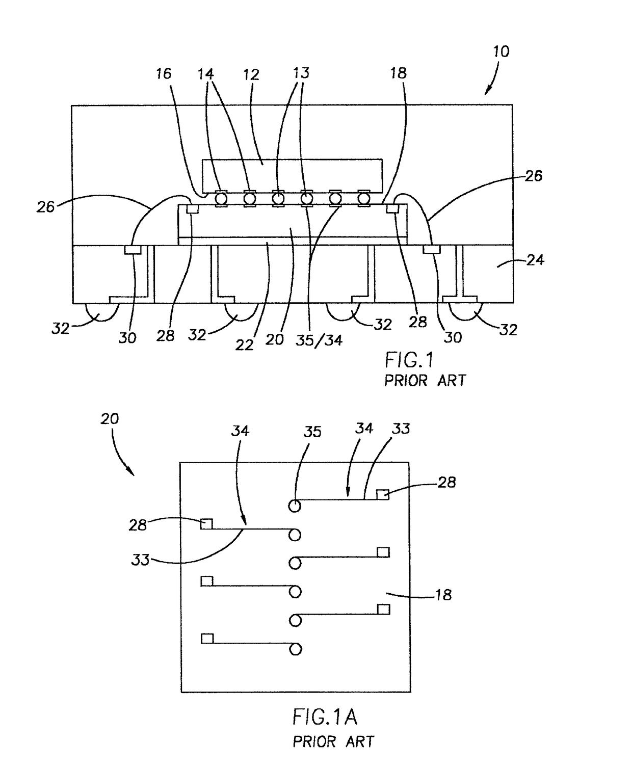
However, if the pitch of the bond pads 13 is tight, it may not be possible to wafer bump the bond pads 13 (e.g., by stencil printing, electrolytic plating, etc), and additional RDL processing on the flip chip die 12 itself may be required.
Fabricating an FC-on-chip can also lead to high costs and process difficulties.
Another drawback is that damage can occur to the active surface 18 of the bottom die 20 during an underfilling process onto the active surface 18, and a molding filler can fail to flow into voids between the dies if the gap is too small.

Method used


Image

  • Elimination of RDL using tape base flip chip on flex for die stacking
  • Elimination of RDL using tape base flip chip on flex for die stacking
  • Elimination of RDL using tape base flip chip on flex for die stacking

Examples


Embodiment Construction

[0028]The invention will be described generally with reference to the drawings for the purpose of illustrating embodiments only and not for purposes of limiting the same. The figures illustrate processing steps for use in fabricating semiconductor devices in accordance with the present invention. It should be readily apparent that the processing steps are only a portion of the entire fabrication process.

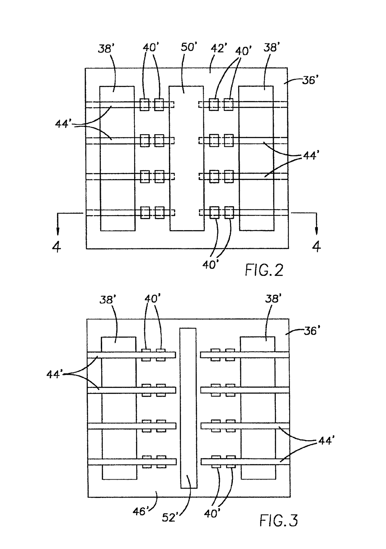
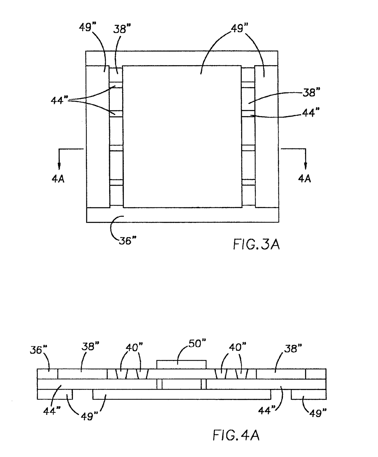
[0029]The invention provides a flexible film interposer for stacking a tape base flip chip onto a second (bottom) die. Recesses are fabricated in the flexible film interposer for the first level interconnect using conventional die mount equipment. The flexible film interposer includes features to interconnect to the second die without the need for an RDL on the second die.

[0030]Referring to FIGS. 2-4, an embodiment of a flexible film interposer 36′ according to the invention is depicted in a simplified top plan view. The flexible film interposer 36′ can be formed from known insulatin...


PUM

PropertyMeasurementUnit
Lengthaaaaaaaaaa
Lengthaaaaaaaaaa
Lengthaaaaaaaaaa

Abstract

A flexible film interposer for stacking a flip chip semiconductor die onto a second (bottom) semiconductor die, semiconductor devices and stacked die assemblies that incorporate the flexible film interposer, and methods of fabricating the devices and assemblies are provided. The incorporation of the flexible film interposer achieves densely packaged semiconductor devices, without the need for a redistribution layer (RDL).

Description

FIELD OF THE INVENTION[0001]This invention generally relates to assembling and packaging multiple semiconductor dies, and more particularly to a stacked multiple die device and methods for fabricating the device.BACKGROUND OF THE INVENTION[0002]Chip-on-board and board-on-chip (BOC) techniques are used to attach semiconductor dies to an interposer or other carrier substrate such as a printed circuit board (PCB). Attachment can be achieved through flip chip attachment, wirebonding, or tape automated bonding (“TAB”).[0003]Flip chip attachment typically utilizes ball grid array (BGA) technology. The BGA component (die) includes conductive external contacts, typically in the form of solder balls or bumps, arranged in a grid pattern on the active surface of the die, which permit the die to be flip chip mounted to an interposer or other carrier substrate (e.g., PCB).[0004]In a flip chip attachment, the balls of the BGA component are aligned with terminals on the carrier substrate, and conn...

Claims


Application Information

Patent Timeline
IPC IPC(8): H01L23/48H01L29/40H01L21/44H01L21/98H01L23/12H01L23/13H01L23/14H01L23/498H01L25/065H05K1/00H05K3/34H05K7/02H05K7/06H05K7/08
CPCH01L23/5387H01L25/0657H01L25/50H01L23/4985H01L23/13H01L2224/48091H01L2924/15311H01L2924/01078H01L2924/01029H01L2225/0651Y10T29/49121H01L2225/06579H01L2224/16237H01L2225/06517H01L2224/48227H01L2225/06527H01L24/48H01L2224/731H01L2224/73204Y10T29/49144H01L2225/06572H01L2224/48465H01L21/56H01L2224/73265H01L2224/32225H01L2924/01322H01L2224/16145H01L2924/01079H01L2924/00014H01L2924/00H01L2924/00012H01L2924/12042H01L24/73H01L2224/05599H01L2224/45099H01L2224/85399H01L2924/14H01L2924/181H01L2224/73253H01L2224/32145H01L2224/48H01L2224/023H01L2224/45015H01L2924/207H01L2224/16225H01L2924/0001
Inventor LEE, TECK KHENG
Owner MICRON TECH INC
Learn More