
Solid-state image pickup apparatus having a hermetic seal portion and fabricating method thereof

Inactive Publication Date: 2006-10-24
OLYMPUS CORP
View PDF11 Cites 13 Cited by
  • Summary
  • Abstract
  • Description
  • Claims
  • Application Information

AI Technical Summary

Benefits of technology

[0013]To eliminate the above problems, it is a main object of the present invention to provide a solid-state image pickup apparatus which can be packaged in a relatively small size while an improved throughput is achieved by saving the time to be spent for wire bonding and at the same time which has a hermetic seal portion readily capable of electrical connection to an external terminal.

Problems solved by technology

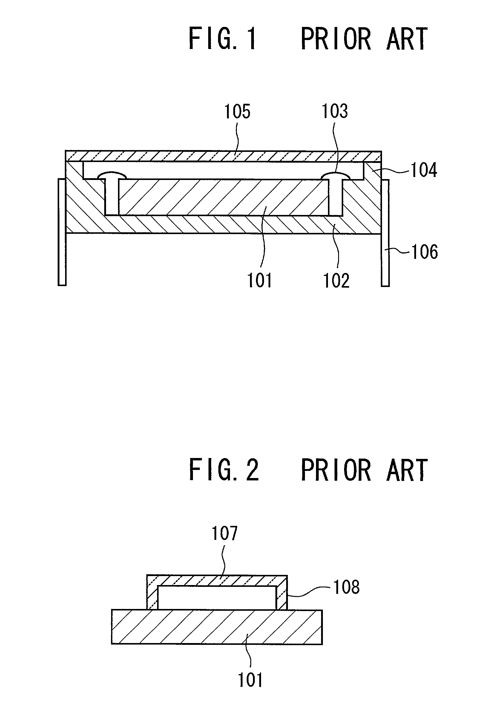
In solid-state image pickup apparatus having such construction, use of package 102 and glass lid 105 for hermetically sealing the entire solid-state image pickup device chip resulted in an increased packaging size and thus had been difficult to be applied to the fields where smaller package size was required.
The previously proposed solid-state image pickup apparatus as described above, however, has the following problems to be solved.
Precision in processing is thus required and difficulties such as an increased amount of work in fabrication are foreseen.
There is thus a problem that the number of processing steps is increased.
Furthermore, a more serious problem presumably occurs with this technique when the solid-state image pickup apparatus has a micro-lens.
If etching is performed before the curing of the resin, however, the resin capable of becoming the frame portion is also etched away similarly as the portion of resin to be removed and there is a possibility that a sufficient frame is not formed.
If etched after the curing of the resin, on the other hand, though a desired shape for the frame is formed, there is a possibility that the micro-lens is etched away at the same time of the etching of the unnecessary portion of resin to be removed due to the fact that the micro-lens is also made of a resin.
An increased number of I / O terminals in the solid-state image pickup device chip results in an increase in the processing time of wire bonding for the I / O pad (terminals) and affects the throughput.
As the above, those previously proposed are with various problems in the construction of hermetic seal portion, even though smaller size packaging is possible and hermetic seal portions can be formed at once for all chips in the form of a wafer.

Method used


Image

  • Solid-state image pickup apparatus having a hermetic seal portion and fabricating method thereof
  • Solid-state image pickup apparatus having a hermetic seal portion and fabricating method thereof
  • Solid-state image pickup apparatus having a hermetic seal portion and fabricating method thereof

Examples


Embodiment Construction

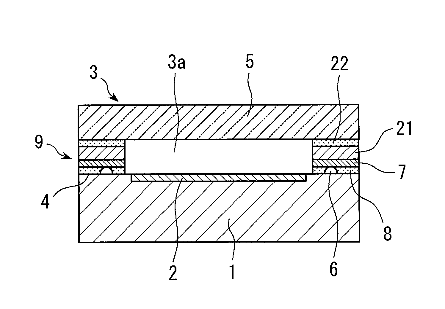
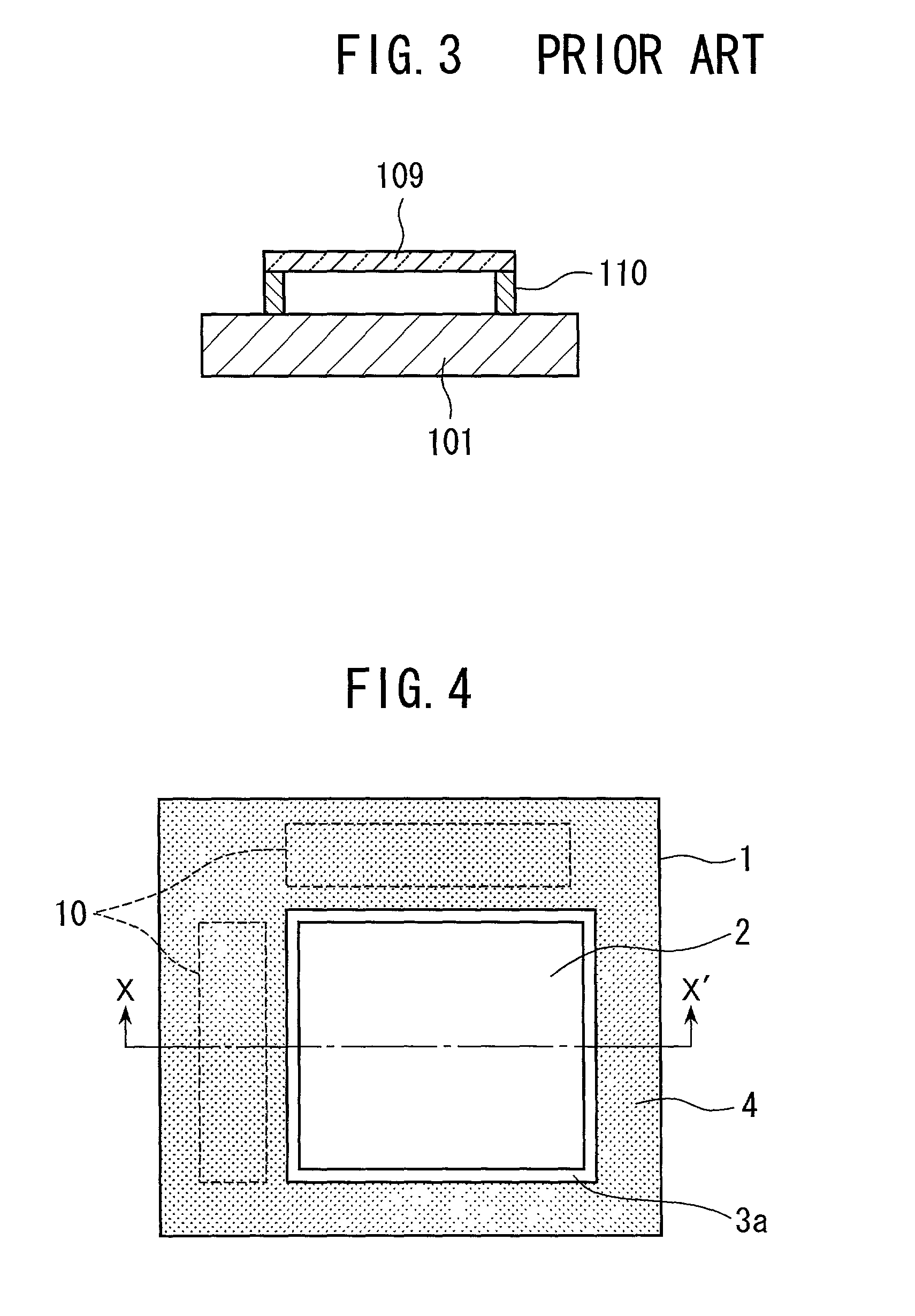
[0043]Some embodiments according to the invention will now be described. First, a first embodiment of the invention will be described below. FIG. 4 is a top view of a solid-state image pickup apparatus according to the first embodiment and FIG. 5 is a sectional view along line X–X′ of FIG. 4. Referring to FIGS. 4 and 5, denoted by numeral 1 is a solid-state image pickup device chip; a bump 6 is formed on an I / O pad of the solid-state image pickup device chip 1. Bump 6 is electrically connected to a metal wiring 7 formed at a side portion of the lower surface of a flat-plate portion 5 consisting of a transparent member which is placed on the top of the solid-state image pickup device chip 1. Here, metal wiring 7 is the wiring for bringing out electrical signals from the I / O pad portion of the solid-state image pickup device chip 1 and it is an equivalent to what can be obtained by extending the I / O pad portion. Those which can be used as the material of metal wiring 7 include aluminu...


PUM


Abstract

A solid-state image pickup apparatus having over solid-state image pickup device chip a hermetic seal portion comprising a flat-plate portion of a transparent member and a frame portion formed on a side portion of a lower surface of the flat-plate portion, said frame portion including a metal wiring, a bump formed on said solid-state image pickup device chip and electrically connected to the metal wiring, and a sealing region for sealing the periphery of the bump by a sealing material, thereby achieving the solid-state image pickup apparatus capable of being packaged in a relatively small size and capable of improving throughput and at the same time having a hermetic seal portion which can be readily electrically connected to an external terminal.

Description

[0001]This application claims benefit of Japanese Application No. 2001-29508 filed in Japan on Feb. 6, 2001, the contents of which are incorporated this reference.BACKGROUND OF THE INVENTION[0002]The present invention relates to solid-state image pickup apparatus and fabricating method thereof having a solid-state image pickup device chip packaged in CSP (chip size package), and more particularly relates to the construction and fabricating method of hermetic seal thereof.[0003]In recent years, there has been an advancement in size reduction for example mainly of portable equipment and, as a result, a further downsizing is demanded also of the casing and inner circuit board therefor. Of those parts to be mounted on a circuit board, semiconductor devices are not excepted from such demands for downsized equipment, and their reduction in size is also required. The same can be said about solid-state image pickup devices which are among the semiconductor devices.[0004]A packaging system a...

Claims


Application Information

Patent Timeline
IPC IPC(8): H04N5/225H01L27/14H01L23/02H04N5/335H04N5/369
CPCH01L27/14618H01L2224/48091H01L2924/00014
Inventor NAKAMURA, TSUTOMUHOSOKAI, SHIGERUMIYATA, KENJI
Owner OLYMPUS CORP
Learn More