
Analog-digital converter using clock boosting

a clock-boosting and analog-digital converter technology, applied in analogue/digital conversion, physical parameter compensation/prevention, instruments, etc., can solve the problems of low power, low voltage analog-digital converters, single chips, etc., and achieve the effect of improving the characteristics of sample-and-hold amplifiers

Inactive Publication Date: 2006-10-24
LG ELECTRONICS INC
View PDF3 Cites 5 Cited by
  • Summary
  • Abstract
  • Description
  • Claims
  • Application Information

AI Technical Summary

Benefits of technology

This design reduces unit costs, maintains input impedance, and improves noise characteristics, enabling high-speed, high-resolution analog-digital conversion without the need for mixers, thus enhancing the operational performance of digital television reception systems.

Problems solved by technology

Furthermore, as the demand for portable equipment is increasing, low power, low voltage analog-digital converters, each of which, together with another Complimentary Metal-Oxide Semiconductor (CMOS) that uses a 1.8 V level low voltage source, can be implemented in a single chip, is under great demand.
Accordingly, this method is disadvantageous in that the unit cost of a digital television board is high because the method should employ a two-stage mixer.
Additionally, the circuit of the method is disadvantageous in that, when a very high input frequency enters in the case where the circuit is used in a sub-sampling analog-digital converter, the operational characteristics of sampling results are deteriorated due to the increase and variation of input impedance, thus causing reduction in performance.
Accordingly, it is difficult to obtain a signal of more than 8 bits.
As a result, it is difficult to use the circuit of the method in a sub-sampling analog-digital converter.

Method used


Image

  • Analog-digital converter using clock boosting
  • Analog-digital converter using clock boosting
  • Analog-digital converter using clock boosting

Examples


Embodiment Construction

[0023]Reference now should be made to the drawings, in which the same reference numerals are used throughout the different drawings to designate the same or similar components.

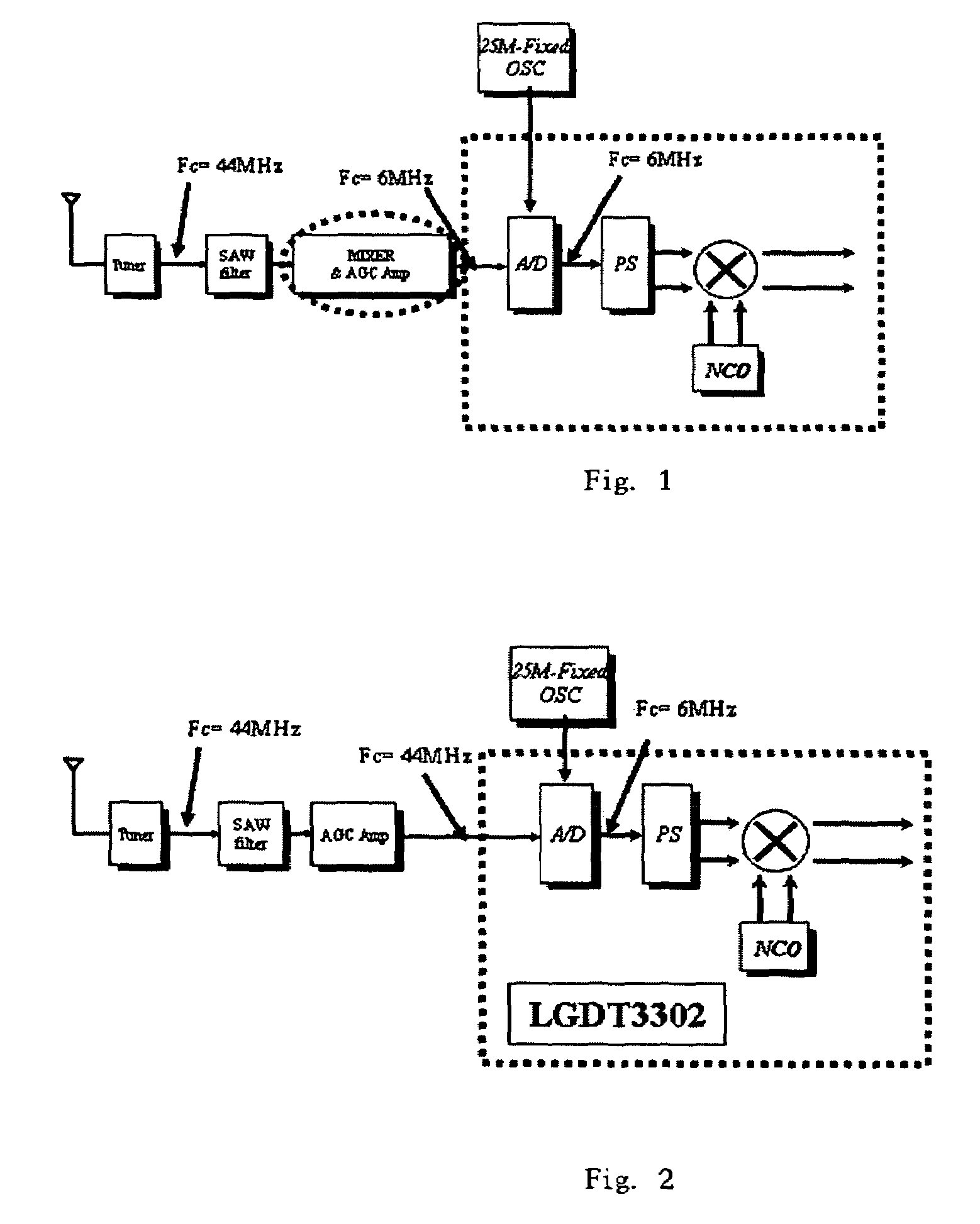
[0024]FIG. 2 illustrates a method of sampling an analog signal to produce an input for an analog-digital converter in which the mixer in FIG. 1 is not employed.

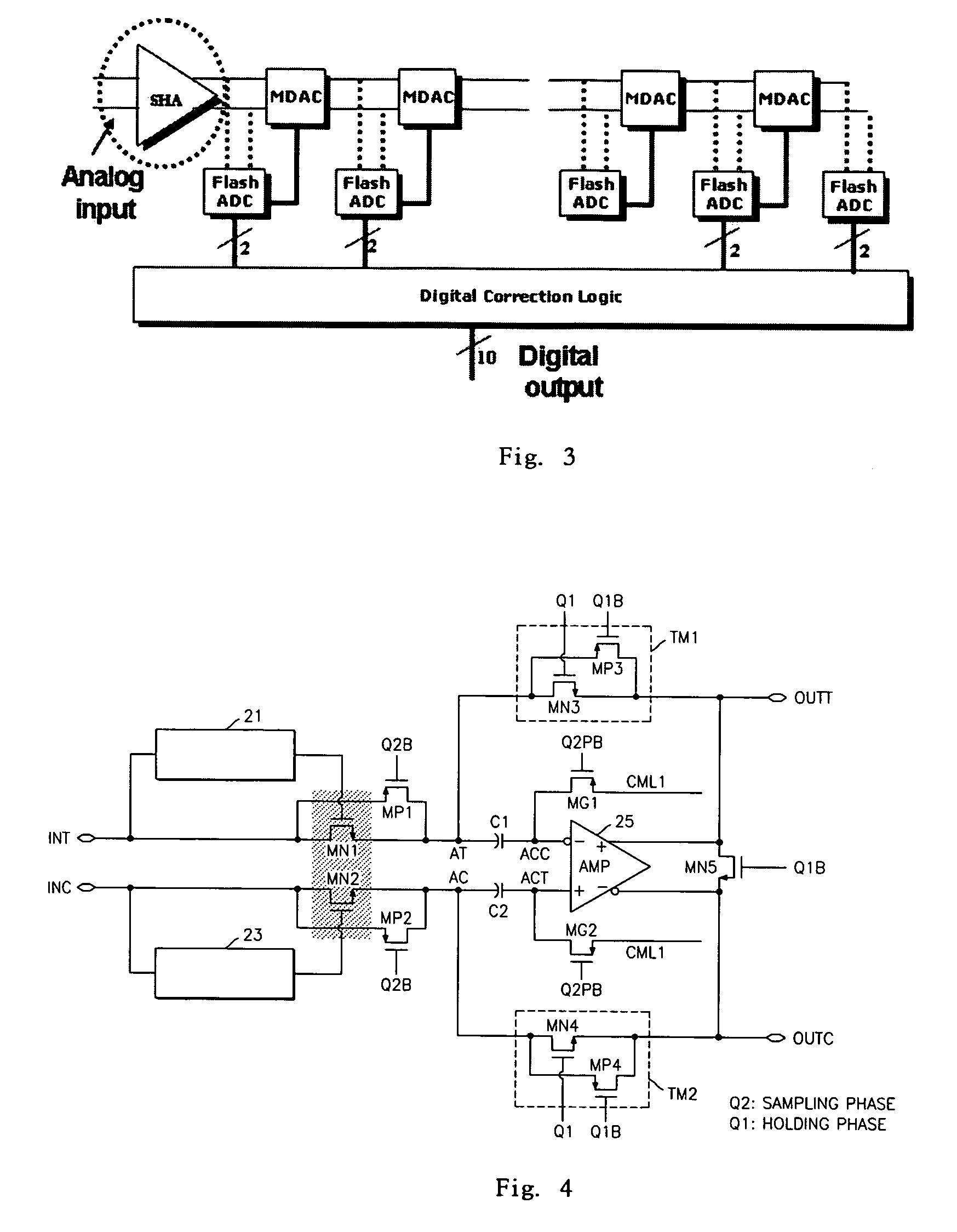
[0025]FIG. 3 is an overall block diagram of an analog-digital converter according to an embodiment of the present invention.

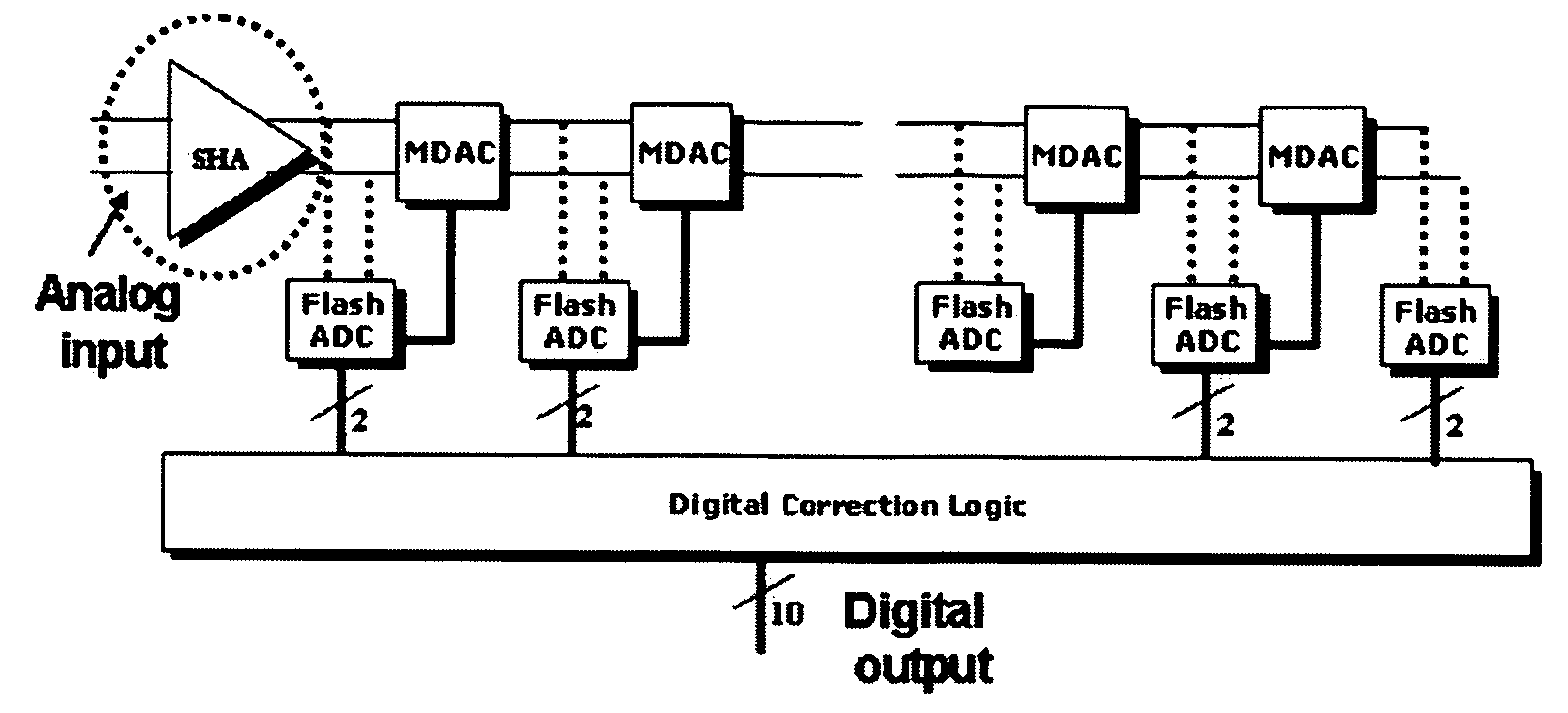
[0026]Referring to FIG. 3, the analog-digital converter according to the present invention has a pipeline structure that acquires two bits from each of a plurality of stages, and includes a sample-and-hold amplifier (SHA) 101, a multiple digital-analog converter 103, a plurality of flash analog-digital converters 102 and a Digital Correction Logic (DCL) 104.

[0027]The analog-digital converter of the present invention employs two clocks, which do not overlap each other, to convert an analog input signal into digital output code.

[0028...


PUM


Abstract

Disclosed herein is an analog-digital converter. The analog-digital converter includes a sample-and-hold amplifier, a first analog-digital converter, a multiple digital-analog converter, a second analog-digital converter, and a digital correction logic. The sample-and-hold amplifier samples an analog input signal using clock boosting. The first analog-digital converter receives a sampled signal, and converts the sampled signal into a plurality of bits of first digital output code. The multiple digital-analog converter receives and stores the sampled signal, and amplifies and outputs the difference between the stored signal and an analog signal corresponding to the first digital output code. The second analog-digital converter receives the output signal of the multiple digital-analog converter, and converts the output signal into a plurality of bits of second digital output code. The digital correction logic receives the first digital output code and the second digital output code, overlaps certain bits of the first digital output code with certain bits of the second digital output code, and outputs remaining bits, exclusive of overlapping bits, as final digital output code.

Description

BACKGROUND OF THE INVENTION[0001]1. Field of the Invention[0002]The present invention relates generally to an analog-digital converter and, more particularly, to a sample-and-hold amplifier using a clock boosting technique and an analog-digital converter having the sample-and-hold amplifier.[0003]2. Description of the Related Art[0004]Recently, with the development of high density Very Large-Scale Integration (VLSI) processing technology and Digital Signal Processing (DSP) technology, the demand for high performance analog-digital converters to be used in high quality video systems, next generation personal portable communication equipment, high speed digital communication networks and medical equipment is gradually increasing. Furthermore, as the demand for portable equipment is increasing, low power, low voltage analog-digital converters, each of which, together with another Complimentary Metal-Oxide Semiconductor (CMOS) that uses a 1.8 V level low voltage source, can be implement...

Claims


Application Information

Patent Timeline
Patent Type & Authority Patents(United States)
IPC IPC(8): H03M1/06H03M1/12H03M1/16
CPCH03M1/1245H03M1/0695H03M1/168H03M1/12
Inventor LEE, WOO-YOL
Owner LG ELECTRONICS INC
Learn More