Package for optical semiconductor device
a technology of optical semiconductors and semiconductor devices, applied in the direction of semiconductor laser structure details, semiconductor lasers, lasers, etc., can solve the problems of high cost, complicated structure, and difficulty in high-speed transmission at 10 gbps or more, and achieve good high frequency characteristics and high frequency characteristics. good
- Summary
- Abstract
- Description
- Claims
- Application Information
AI Technical Summary
Benefits of technology
Problems solved by technology
Method used
Image
Examples
embodiment 1
[0051
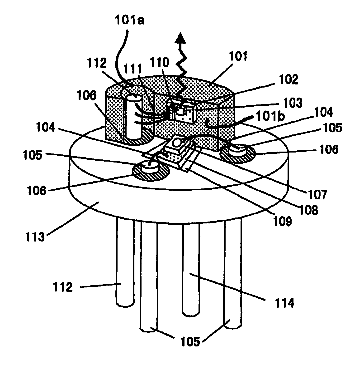
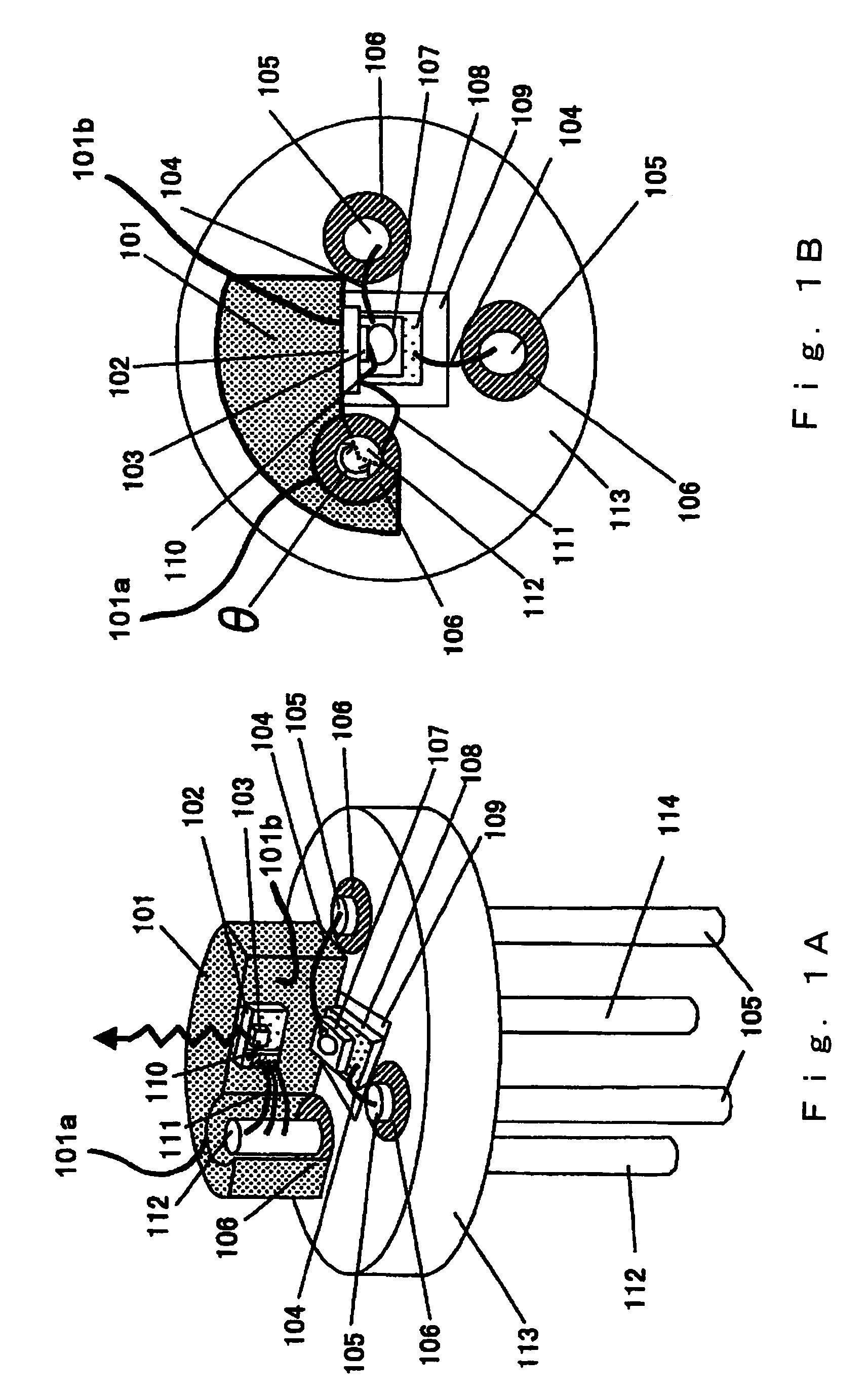
[0052]FIGS. 1A and 1B are a perspective diagram and plane view of the optical semiconductor device of Embodiment 1 concerning this invention.
[0053]The optical semiconductor device of this embodiment 1 is a laser device for optical communications, and is constituted using a package for Optical semiconductor device peculiar to the present invention and Optical semiconductor element such as a laser diode.
[0054]In the optical semiconductor device of this embodiment 1, the package for Optical semiconductor device is similar to the conventional package for Optical semiconductor device in FIG. 9 except that a mount 101 is used instead of the mount 901 in order to make high frequency characteristics good. In addition, in FIG. 1, the same elements as FIG. 9 are attached with the same code.
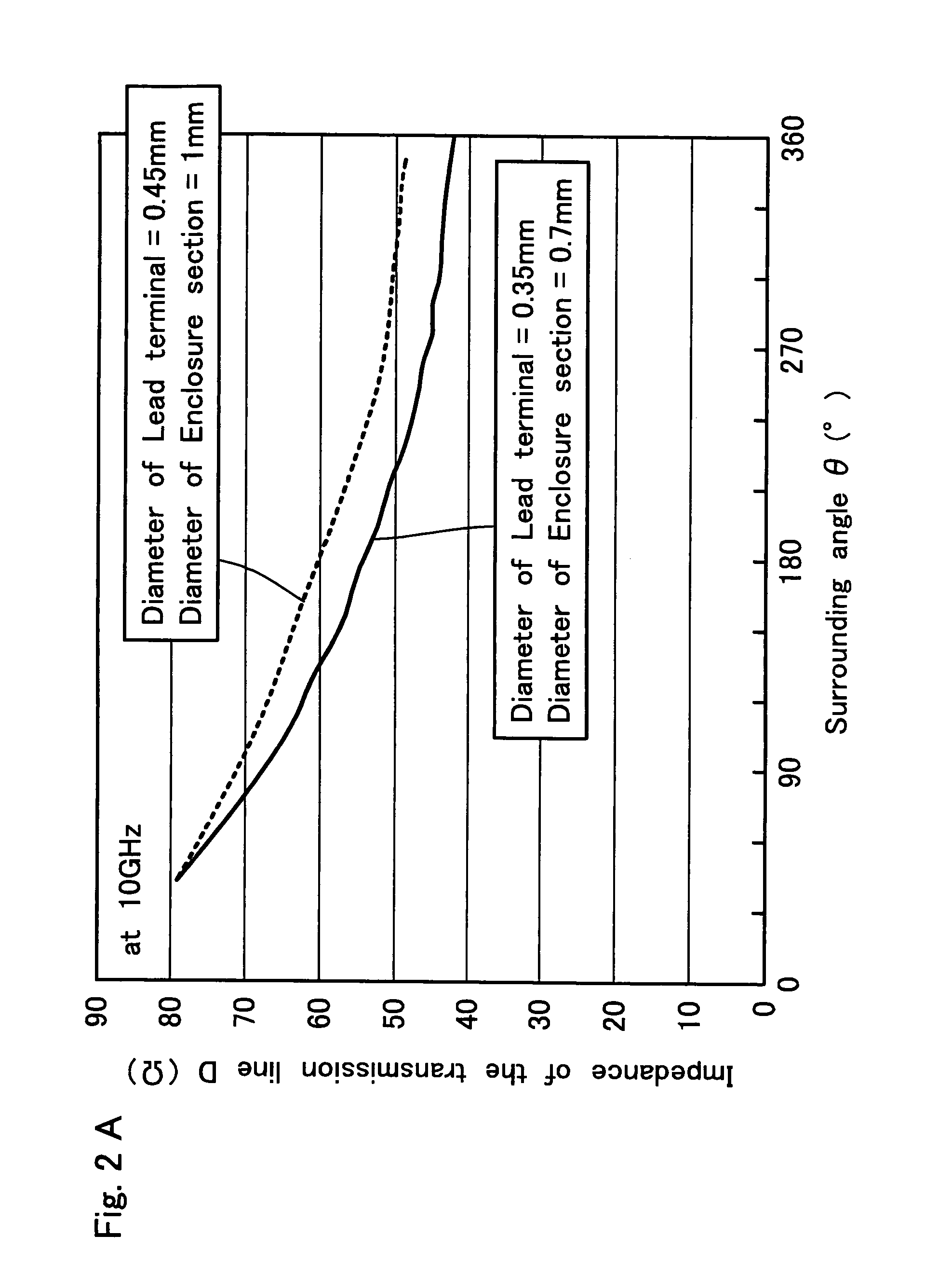
[0055]In the optical semiconductor device of an embodiment 1 , the mount 101 of the package for Optical semiconductor devices has a mount face 101b to be mounted by a laser diode 103 and a circumferenc...
embodiment 2
[0081
[0082]The optical semiconductor device of Embodiment 2 of the present invention is composed using a package for optical semiconductor device with improved high frequency properties as will be described below. To be more specific, as shown in FIG. 3 the package for optical semiconductor device of Embodiment 2 has the same structure as the conventional package for optical semiconductor device shown in FIG. 9 except that in the conventional package the counter earth electrode part 201 made of a conductive member, a dielectric member having a metallized surface or the like is further provided adjacent to the lead terminal for signal supply 112.
[0083]In Embodiment 2, the lead terminal for signal supply 112 and the counter earth electrode part 201 compose the transmission line D, which has lower impedance than in the conventional example shown in FIG. 9.
[0084]The result is a reduction in reflection coefficient between the transmission line C and the transmission line D.
[0085]As descr...
embodiment 3
[0088
[0089]The optical semiconductor device of Embodiment 3 of the present invention is composed using a package for optical semiconductor device with improved high frequency properties as will be described below. To be more specific, as shown in FIG. 4 the package for optical semiconductor device of Embodiment 3 has the same structure as the package for optical semiconductor device of Embodiment 2 except that in the package of Embodiment 2 a dielectric plate 301 (for example, a dielectric member having a relative permittivity of 2 to 12, more specifically made of alumina or the like) is further provided between the counter earth electrode part 201 and the lead terminal for signal supply 112.
[0090]In Embodiment 3, the lead terminal for signal supply 112, the counter earth electrode part 201, and the dielectric plate 301 compose the transmission line D. The relative permittivity of this dielectric plate which is higher than in a vacuum (in the air) enables the transmission line D to ...
PUM
 Abstract
Description
Claims
Application Information
 - R&D
- Intellectual Property
- Life Sciences
- Materials
- Tech Scout
- Unparalleled Data Quality
- Higher Quality Content
- 60% Fewer Hallucinations
Browse by: Latest US Patents, China's latest patents, Technical Efficacy Thesaurus, Application Domain, Technology Topic, Popular Technical Reports.
© 2025 PatSnap. All rights reserved.Legal|Privacy policy|Modern Slavery Act Transparency Statement|Sitemap|About US| Contact US: help@patsnap.com


