Chip-component accommodating device and examining apparatus having the same

a technology of examining apparatus and accommodating device, which is applied in the direction of semiconductor/solid-state device details, manufacturing tools, transportation and packaging, etc., can solve the problems of increasing the cost of the device, the device to be larger in size and more complex, and the device to be further increased

Inactive Publication Date: 2006-09-12
RICOH ELECTRONIC DEVICES CO LTD +2
View PDF5 Cites 2 Cited by
  • Summary
  • Abstract
  • Description
  • Claims
  • Application Information

AI Technical Summary

Benefits of technology

[0014]Accordingly, the general object of the present invention is to provide a chip-component inserting and accommodating device that speeds up packaging of the chip component and enhances inserting stability without significantly increasing the cost of the device.
[0017]Thus, by moving the carrier tape with the upper part of the chip component covered with the tip face of the suction nozzle and the cover, the chip component will not fall out of the component-accommodating recess of the carrier tape or deviate from the normal position even if the carrier tape is moved before the negative pressure of the suction nozzle is completely gone, thus enabling a reliable insertion of the component.
[0018]Furthermore, in comparison to the conventional device, it is only necessary to add a cover and there is no need for a high-accuracy component or a sophisticated assembling technique, and increase in the cost of the device can be more or less avoided.
[0019]Moreover, after the negative pressure of the suction nozzle is released, there is no need to wait until all of the negative pressure is completely gone to move the carrier tape, thus greatly saving packaging time.
[0021]Thus, in the chip-component examining apparatus, the chip component that has undergone an examination process can be packed securely and rapidly, and the chip-component packing process will not be the bottleneck process controlling the operation speed of the entire examining apparatus.

Problems solved by technology

However, in the automatic packaging device disclosed in the Japanese Laid-Open Utility Model Application 5-81004, a push plate that is lowered in sync with the suction nozzle, as well as a mechanism for driving the push plate, are required, thus causing the device to be larger in size and to be more complex, and furthermore causing the cost of the device to increase.
Furthermore, since the push plate and the suction nozzle are lowered synchronously, a high standard in assembling accuracy of the device is also required, causing the cost of the device to further increase.

Method used


Image

  • Chip-component accommodating device and examining apparatus having the same
  • Chip-component accommodating device and examining apparatus having the same
  • Chip-component accommodating device and examining apparatus having the same

Examples


embodiment

[Embodiment]

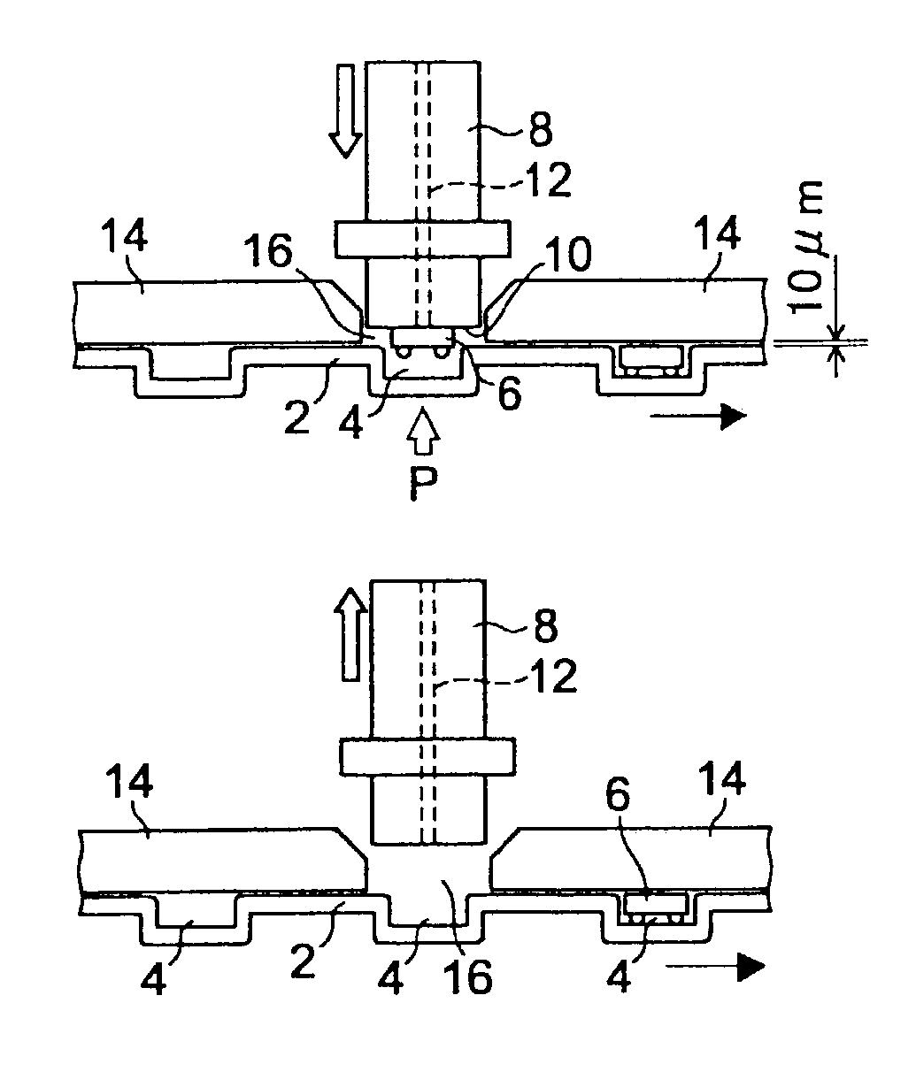
[0047]FIG. 1A shows the main part of one embodiment of the chip-component accommodating device of the present invention. The chip-component accommodating device accommodates the chip component to the tape carrier formed with accommodating recesses and seals it with a covering tape. This type of chip-component accommodating device is sometimes referred to as a taping unit.

[0048]The tape carrier 2 is made of resin and is formed with component-accommodating recesses 4, for accommodating chip components, which recesses are equally spaced apart in a line in the longitudinal direction of the tape carrier. The tape carrier 2 is wound around a reel and supplied therefrom, and is intermittently fed by being unwound from the reel. After accommodating the chip component, the component-accommodating recess 4 is sealed with covering tape, and is subsequently wound to a different reel. A position shown as P is an inserting position for accommodating the chip component, at which positi...


PUM

PropertyMeasurementUnit
Sizeaaaaaaaaaa
Circumferenceaaaaaaaaaa
Vacuumaaaaaaaaaa

Abstract

According to the present invention, in the field of packaging the chip component, increase in speed and stability in packaging the chip component is achieved without significantly increasing the cost of the device. The size of the suction face of the suction nozzle is set so as to be larger than the relevant chip component. Near the inserting position P of the chip component, a push cover is provided in close proximity to the upper surface of the carrier tape. A hole is provided in the push cover at the inserting position P, and the size of the hole is slightly larger than the size of the tip face of the suction nozzle. After the chip component held to the suction nozzle enters the component-accommodating recess of the carrier tape, the suction of the suction nozzle is released and the carrier tape starts to move in the direction shown with an arrow, orthogonal to the suction nozzle. The suction nozzle is raised after the opening of the component-accommodating recess is completely under the push cover.

Description

BACKGROUND OF THE INVENTION[0001]This application claims the benefit of Japanese Patent Application No. 2002-000898 filed Jan. 7, 2002 in the Japanese Patent Office, the disclosure of which is hereby incorporated by reference.[0002]1. Field of the Invention[0003]The present invention relates to a chip-component accommodating device for automatically inserting and accommodating a chip component, for example, a compact chip component such as a chip size package (CSP) of a semiconductor device in an embossed carrier tape in a stable state; and to a chip-component examining apparatus provided with the same.[0004]2. Description of the Related Art[0005]After chip components are tested with respect to electrical properties, in the final manufacturing stage, to determine whether there are defects or not, only the non-defective components are packaged into a predetermined package form and then shipped. Such a task is more or less automatically carried out. Presently, for example, the most co...

Claims


Application Information

Patent Timeline
IPC IPC(8): B23P19/00B65B57/10B65B15/04B65B35/56H01L21/00H01L21/683
CPCH01L21/67144H01L21/6838Y10T29/53261Y10T29/53174Y10T29/53178H01L24/75H01L24/81H01L24/97H01L2224/16225Y10T83/8789
Inventor NAKAGAWA, JUNICHIINOUE, YUUJI
Owner RICOH ELECTRONIC DEVICES CO LTD
Why Eureka
Try Eureka