
Flash memory device and program verification method thereof

a flash memory and program verification technology, applied in static storage, digital storage, instruments, etc., can solve the problems of premature end of program operation, non-uniform distribution of threshold voltage (vt) at the high end, and overprogramming of flash memory cells of page units

Active Publication Date: 2006-08-29
SAMSUNG ELECTRONICS CO LTD
View PDF13 Cites 18 Cited by
  • Summary
  • Abstract
  • Description
  • Claims
  • Application Information

AI Technical Summary

Benefits of technology

[0012]There is a demand for a flash memory device and a program verification method thereof, which can prevent a misjudgment as to whether the flash memory cells are programmed or not.
[0013]Accordingly, embodiments of the present invention provide a flash memory device and a program verification method which can prevent a misjudgment as to whether flash memory cells are programmed or not. Additionally, embodiments of the invention are able to provide a substantially uniform distribution of the threshold voltage across programmed memory cells.

Problems solved by technology

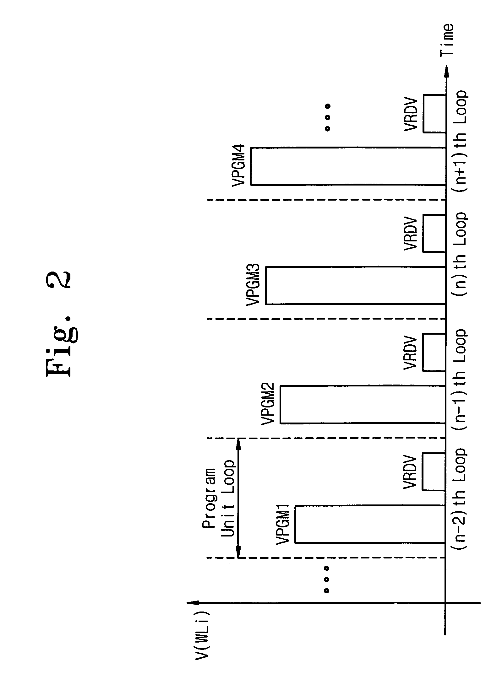
If the program operation and the program verification operation are repeatedly performed to one selected word line, a problem may be caused where the programming operation is prematurely ended by misjudging underprogrammed flash memory cells as programmed.
As a result, the threshold voltage (Vt) is distributed non-uniformly at the high end.
This non-uniform distribution of the high threshold voltage (Vt) causes a problem of overprogramming the flash memory cells of the page unit.
Additionally, the flash memory cells having a low threshold voltage (Vt), similar to the program verification voltage VRDV, may remain in an underprogrammed state because it is uncertain whether the flash memory cells are programmed or not.

Method used


Image

  • Flash memory device and program verification method thereof
  • Flash memory device and program verification method thereof
  • Flash memory device and program verification method thereof

Examples


Embodiment Construction

[0025]Reference will now be made in detail to embodiments of the present invention, examples of which are illustrated in the accompanying drawings. However, the present invention is not limited to the embodiments illustrated hereinafter, and the embodiments herein are rather introduced to provide easy and complete understanding of the scope and spirit of the present invention.

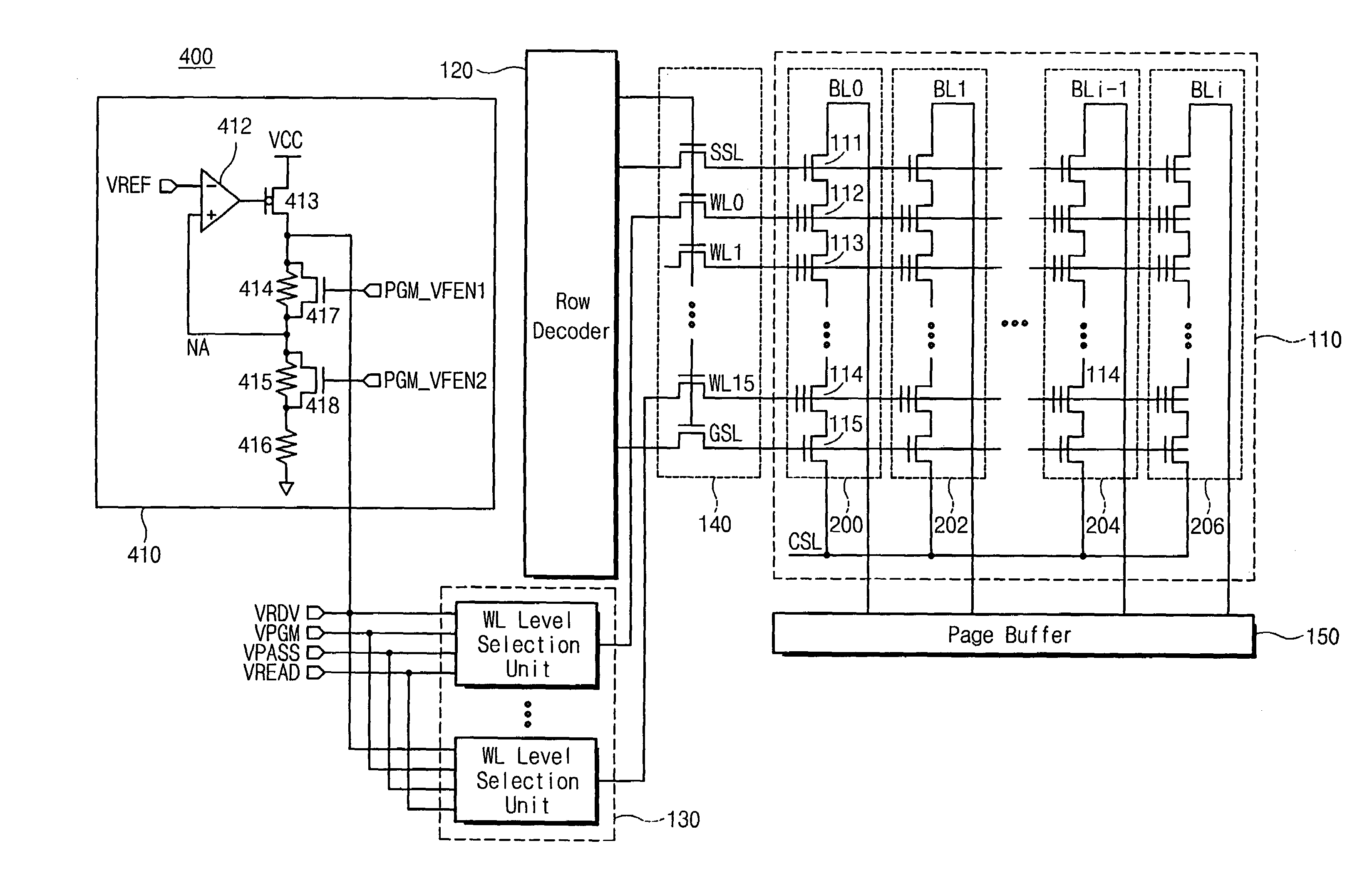
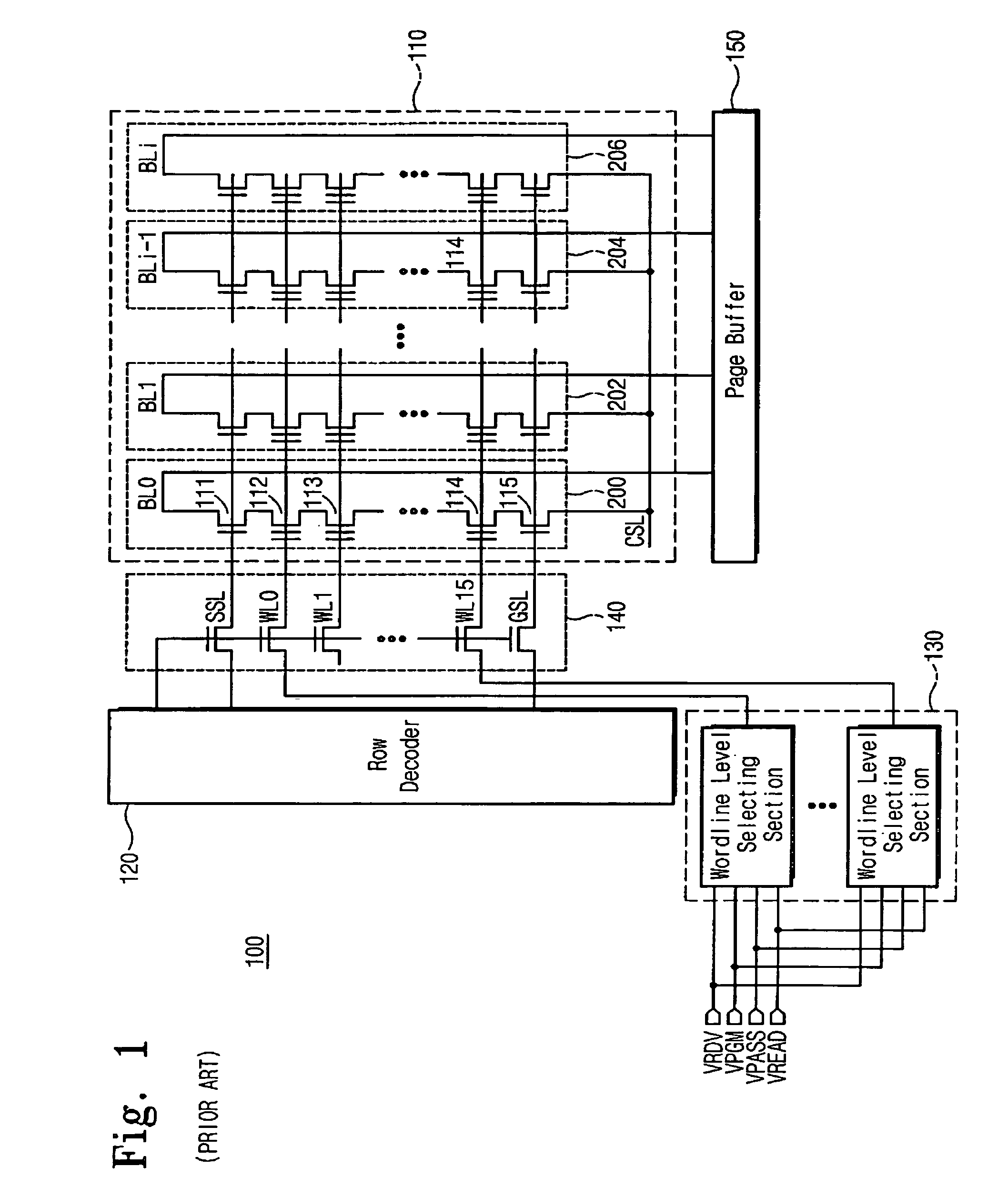
[0026]FIG. 4 is a view of a flash memory device according to an embodiment of the present invention. Compared with the conventional flash memory device of FIG. 1, the flash memory device 400 further includes a program verification voltage generator 410. The program verification voltage generator 410 includes a PMOS transistor 413 connected to a power supply voltage VCC, a first NMOS transistor 417 connected to both terminals of a first resistor 414, a second NMOS transistor 418 connected to both terminals of a second resistor 415, and a third resistor 416 connected from the second NMOS transistor 418 to a groun...


PUM


Abstract

Disclosed is a flash memory device and a program verification method thereof which can prevent a misjudgment as to whether flash memory cells are programmed or not. The flash memory device includes: a program verification voltage generator for variably generating program verification voltages used to verify whether the flash memory cells are programmed or not and a word line level selector for transferring the program verification voltages to word lines connected to control gates of the flash memory cells. The flash memory cells that are verified as uncertain as to whether the flash memory cells are programmed or not can be completely programmed since the program verification operation is carried out with program verification voltage levels that are changed according to the selective activations of the program verification control signals.

Description

[0001]This application claims priority from Korean Patent Application No. 2002-71599, filed on Nov. 18, 2002, the contents of which are herein incorporated by reference in their entirety.TECHNICAL FIELD[0002]This disclosure relates to a semiconductor memory device, and more particularly, to a flash memory device that uses variable program verification voltages.BACKGROUND[0003]A flash memory device is a nonvolatile high-density data storage device that can write and erase data on-board. A flash memory cell includes a field effect transistor (FET) having a selection gate, a floating gate, a source and a drain. Data is stored in the flash memory cell by variations in the amount of charge stored in the floating gate, which causes a variation in a threshold voltage (Vt) of the flash memory cell. The data stored in the flash memory cell is read out by applying a selection voltage to a word line connected to the selection gate. The amount of current, which flows when the flash memory cell ...

Claims


Application Information

Patent Timeline
Patent Type & Authority Patents(United States)
IPC IPC(8): G11C16/34G11C11/34G11C16/02G11C16/00G11C16/04G11C16/06G11C16/30
CPCG11C16/3454G11C16/0483G11C16/30G11C16/00
Inventor SUH, KANG-DEOGLEE, YEONG-TACKLEE, JIN-WOOK
Owner SAMSUNG ELECTRONICS CO LTD
Learn More