
Coaxial via structure for optimizing signal transmission in multiple layer electronic device carriers

a technology of electronic device carrier and via structure, which is applied in the direction of printed element electric connection formation, waveguide, high frequency circuit adaptation, etc., can solve the problems of unexpected low performance, insufficient control of impedance, and inability to predict the propagation of electromagnetic waves

Inactive Publication Date: 2006-08-15
IBM CORP
View PDF5 Cites 31 Cited by
  • Summary
  • Abstract
  • Description
  • Claims
  • Application Information

AI Technical Summary

Benefits of technology

[0016]An object of the invention to provide a tr...

Problems solved by technology

It is known that even if a material and a module structural configuration are defined there still may be unexpected low performance.
It has been proven by simulation and measurements that propagation of an electromagnetic wave can also be severely affected by many kinds of discontinuities along its propagation path.
These discontinuities can translate into electrical impedance (Z0) mismatches that are known to cause reflections of the signal.
Controlling the impedance may not be sufficient due to the presence of other structures called parasitic elements (that may be capacitive, inductive and resistive) that become embedded within the package by the association of materials and electrical structures.
These parasitic elements have very negligible effects in low speed digital applications but they can severely affect the signal propagation in high speed applications.
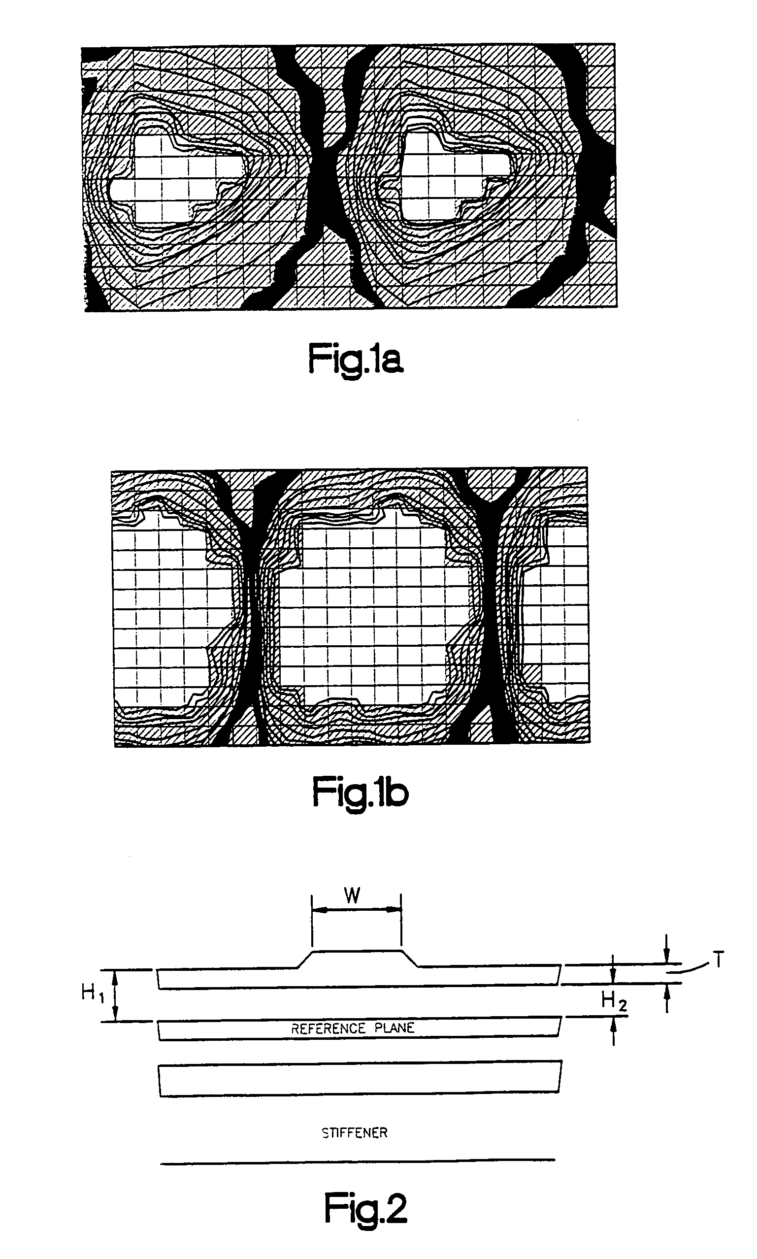
The more the “eye” closes, as illustrated on FIG. 1, the more difficult it is to determine whether switching transition has taken place or if the shift of the signal baseline is due to background noise.
Such a combination acts, at high frequencies, as a low pass filter and therefore reduces the transmission line bandwidth.
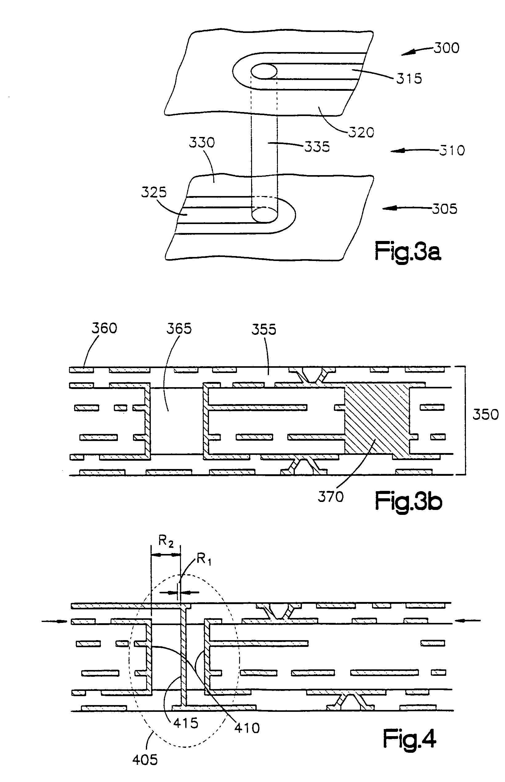
Unfortunately the traditional vertical transition (PTH) does not have the possibility to offer the same referenced structure with the current standard processes in place today.

Method used


Image

  • Coaxial via structure for optimizing signal transmission in multiple layer electronic device carriers
  • Coaxial via structure for optimizing signal transmission in multiple layer electronic device carriers
  • Coaxial via structure for optimizing signal transmission in multiple layer electronic device carriers

Examples


Embodiment Construction

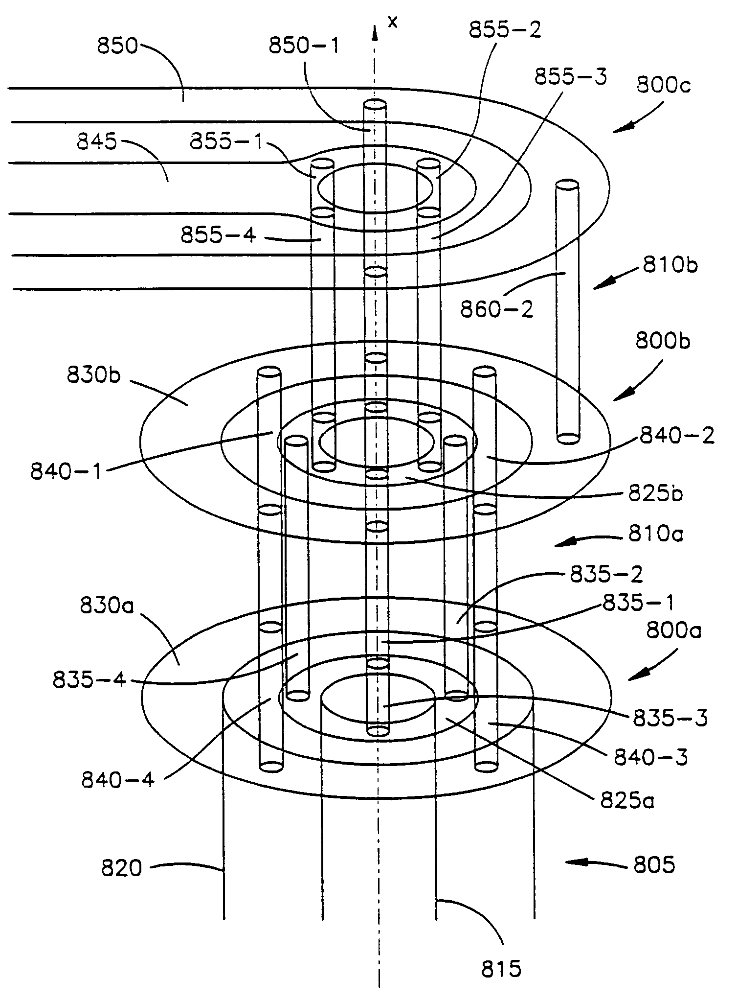
[0031]According to the invention there is provided a coaxial via structure that may be implemented in an electronic device carrier comprising several conductive layers. Such coaxial via structure can deliver a referenced shielding element to a high speed line between conductive layers making it possible to be in compliance with geometry requirements to achieve a controlled impedance along this transition. The laminate electronic device carrier comprising the coaxial via structure according to the invention can be processed through standard manufacturing operations.

[0032]FIG. 4 illustrates a partial cross section view of an electronic device carrier illustrating an embodiment of the coaxial via structure of the invention. In this example, the electronic device carrier is based on a 2S2P core 400 that comprises two internal conductive layers and a conductive layer on each side that are covered with a dielectric material, e.g. epoxy, on which external conductive tracks may be designed,...


PUM

PropertyMeasurementUnit
Timeaaaaaaaaaa
Thicknessaaaaaaaaaa
Structureaaaaaaaaaa

Abstract

A coaxial via structure is adapted to transmit high speed signals or high intensity current through conductive layers of an electronic device carrier. The coaxial via structure comprises a central conductive track and an external conductive track separated by a dielectric material and is positioned in a core of the electronic device carrier or in the full thickness of the electronic device. The coaxial via structure can be combined with a stacked via structure so as allow efficient transmission of high speed signals across the electronic device carrier when a manufacturing process limits the creation of a full coaxial via structure across the entire electronic device carrier.

Description

FIELD OF THE INVENTION[0001]The present invention relates generally to the structure and manufacture of electronic printed circuit boards and chip carriers and more specifically to a particular structure of conductive tracks in multiple layer high density electronic device carriers.BACKGROUND OF THE INVENTION[0002]Electronic packages used in high speed applications have an important function beyond the classical mechanical protection for the semiconductor devices that are packaged thereon. These types of packages should maintain semiconductor device performance during operation. When the switching speed of the devices goes above the 1 Gigahertz (GHz) clock rate, there is the need to consider the transmission of an electrical signal as the propagation of an electromagnetic wave, supported by current in a circuit trace, as a performance factor. This electromagnetic wave propagation is affected by the electronic packaging material properties such as dielectric constant as well as diele...

Claims


Application Information

Patent Timeline
IPC IPC(8): H01R12/04H05K1/11H01P1/04H01P3/06H05K1/02H05K3/42H05K3/46
CPCH01L23/66H01P1/047H01P3/06H05K1/0222H05K1/115Y10T29/49165H05K1/0251H05K3/429H05K3/4602H05K2201/09618H05K2201/09627H05K2201/09809H01L2924/0002H01L2924/3011Y10T29/49117Y10T29/49126H01L2924/00
Inventor OGGIONI, STEFANO S.ROGIANI, GIANLUCASPREAFICO, MAUROVIERO, GIORGIO
Owner IBM CORP
Learn More