Coupling device

a technology of couplers and couplers, which is applied in the direction of electrical equipment, multiple-port networks, waveguides, etc., can solve the problems of compromising the circuit area, the coupler will not perform properly, and the use of couplers in the 1-5 ghz range has been at the expense of a large area of occupation

Inactive Publication Date: 2006-08-01
NOKIA CORP
View PDF8 Cites 43 Cited by
  • Summary
  • Abstract
  • Description
  • Claims
  • Application Information

AI Technical Summary

Benefits of technology

[0028]Consequently, it is an object of the present invention to provide a coupling device which is free from such drawbacks due to a degradation of Zoe.
[0037]Accordingly, with the present invention being implemented to a coupling device, the following advantages can be achieved:
[0038]The degradation of Zoe is compensated for with the use of one or more of the short-circuit stubs connected to the coupled line, e.g. introduced at the centre thereof. By compensating for Zoe using the stubs and further by compensating for Ve\Vo mismatch using capacitors to ground, significant improvements to the performance of the coupler can be achieved.
[0040]The novel compensated technique according to the present invention that has been suggested enables the use of Broadside Coupled Line components embedded in Multilayer Structures. The technique enables a high performance combined with miniaturised size and reduced substrate thickness, and offers in this way the best of all possible design scenario in terms of wideband performance; reduced size; and reduced cost.

Problems solved by technology

The use of couplers in the 1-5 GHz range though has been at the expense of large area of occupation required for such couplers and fabrication tolerance problems resulting from tight gap dimensioning for 3 dB coupling operation when implemented in PCB technology (PCB=Printed Circuit Board).
More precisely, when implementing a coupler in PCB technology, it is necessary to accurately provide a gap between coupling lines of a coupler with the designed dimensions since otherwise the coupler will not perform properly.
Often SMD component type couplers require additional external matching components to optimise their performance in terms of isolation and matching as well as amplitude and phase balance and therefore even further compromise the circuit area.
Stated in other words, the provision of externally provided SMD components for matching purposes further increases the entire size of the coupler and requires additional soldering processes for soldering the externally provided SMD components.
The increased use of SMD components increases costs and the use of soldering connections compromises the environmental friendliness and reduces the reliability of a manufactured subsystem module since each solder connection represents a potentially source of error.
Stripline technology has also been utilised for the design of high performance couplers but its suffers from the need to accommodate for larger volume / size for a given component inflicting additionally more materials costs.
Low loss performance can also be an issue especially in LNA designs (LNA=Low Noise Amplifier) as well as in high efficiency power amplification and linearisation applications.
Current designs offer typically 0.3 dB loss performance per coupler.
This high-density integration scenario relies on the use of stripline components, which as stated above suffers from an increase in area / volume for a given component inflicting additionally more material costs.
The implementation of stripline couplers carries a significant disadvantage in requiring a much larger thickness of substrate as compared to its microstrip counterpart to achieve similar performance for the same geometry.
Hence when optimising for cost by reducing the number of layers used, the performance of stripline couplers will suffer.
This may be due to size, cost or reliability considerations, or a combination of all.
The reduced Zoe impacts adversely on the amplitude and phase balance of the coupler, as well as on the matching and isolation.
Reducing the transmission line width has an adverse effect on Zoo, which imposes a limit on how much we can ultimately reduce the width and still be able to meet the Zoo requirement.
However if a transmission line is placed in an inhomogenous (and / or non-symmetric) dielectric substrate it can no longer support fully-TEM propagation because the electromagnetic wave-now propagates mostly within the substrate, but some of the wave is now able to propagate in air also.
Meandering introduces structural discontinuities which degrade the performance by introducing asymmetry for the normally symmetrical normal modes of propagation.

Method used


Image

  • Coupling device
  • Coupling device
  • Coupling device

Examples


first embodiment (fig.6)

First Embodiment (FIG. 6):

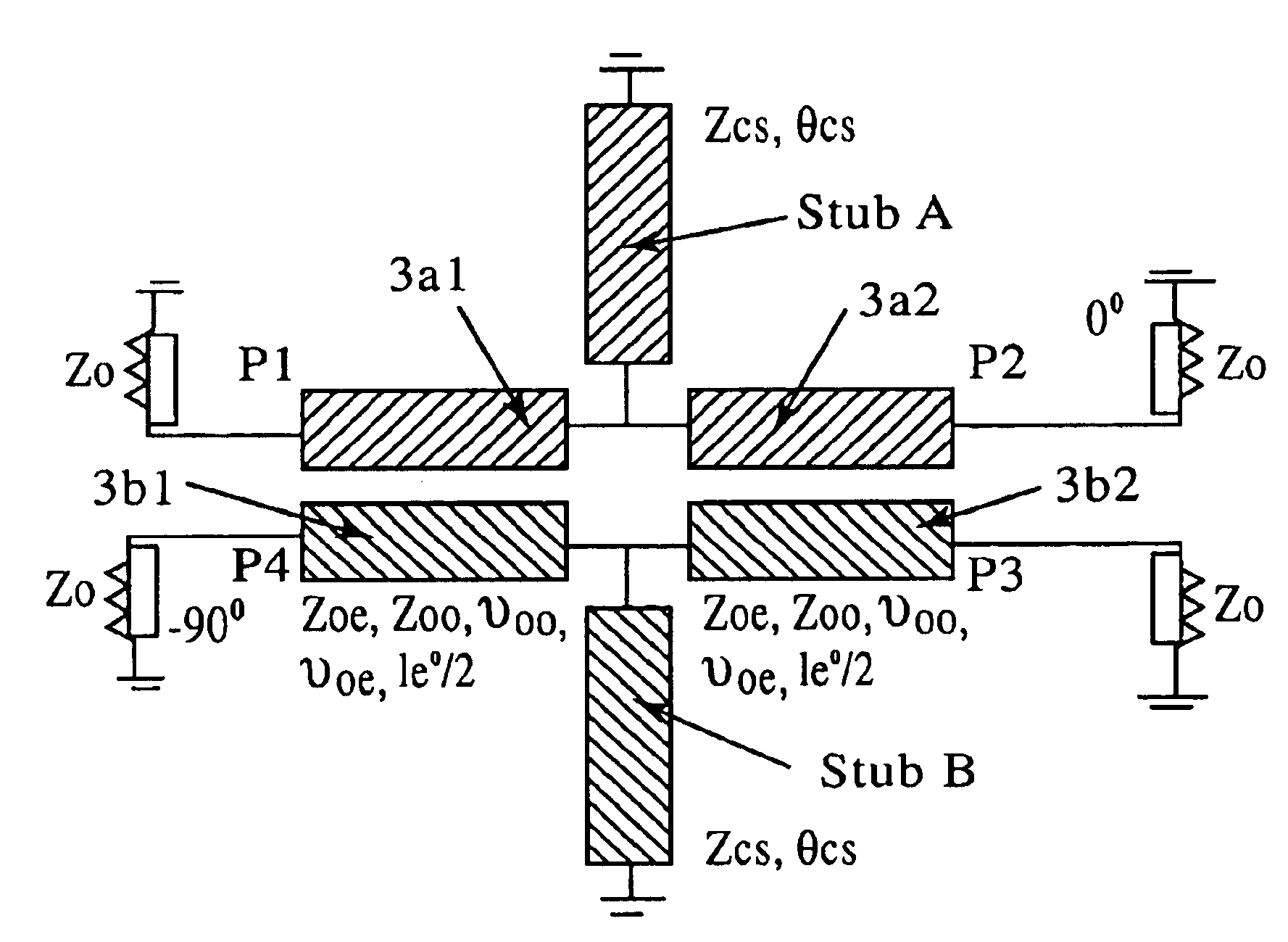
[0062]Considering the first embodiment shown in FIG. 6, said at least one cover layer 4, 5 is covered by a second conductive layer 2′, and at least one short-circuit stub Stub A is connected between at least one of said electromagnetically coupled lines 3b (3b1, 3b2) and said second conductive layer. Stated in other words, two stubs Stub A and Stub B are connected to the arrangement, one stub being connected to a respective one of said coupled lines.

[0063]It is to be noted that in case an even number of electromagnetically coupled lines is provided (as in FIG. 6), the number of short-circuit stubs connected to said first conductive layer 3a (3a1, 3a2) is equal to the number of short-circuit stubs connected to said second conductive layer 3b (3b1, 3b2).

[0064]Furthermore, as shown in FIG. 6, said short-circuit stub and / or stubs is / are connected to an electromagnetically coupled line at half the electrical length of said line (le° / 2). However, this is not nece...

second embodiment (fig.7)

Second Embodiment (FIG. 7):

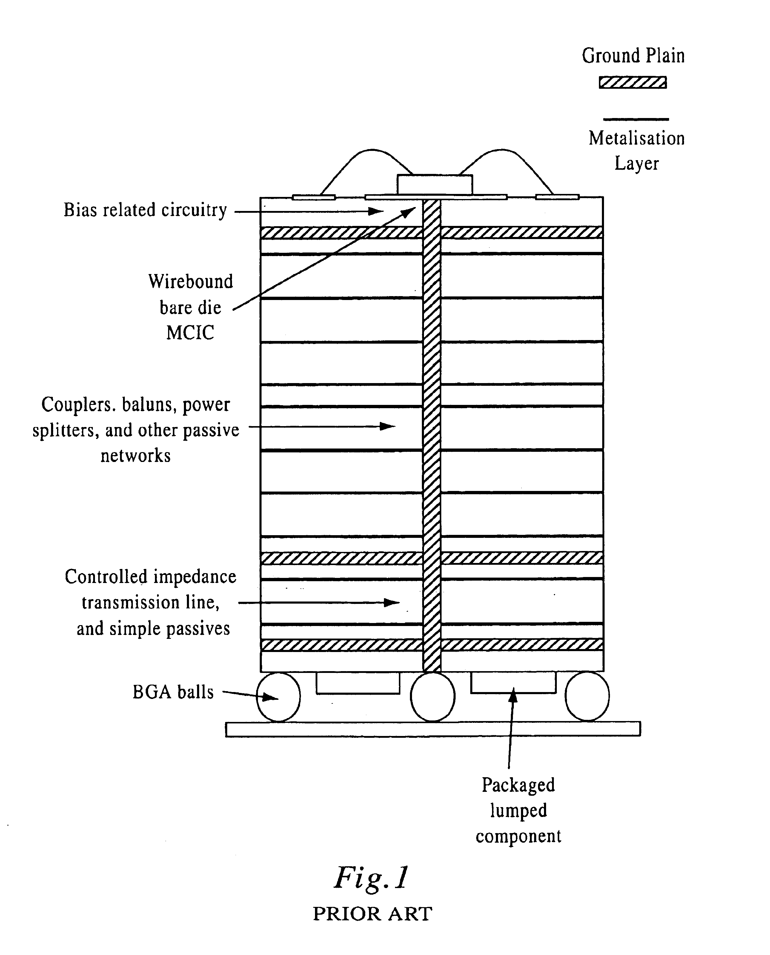
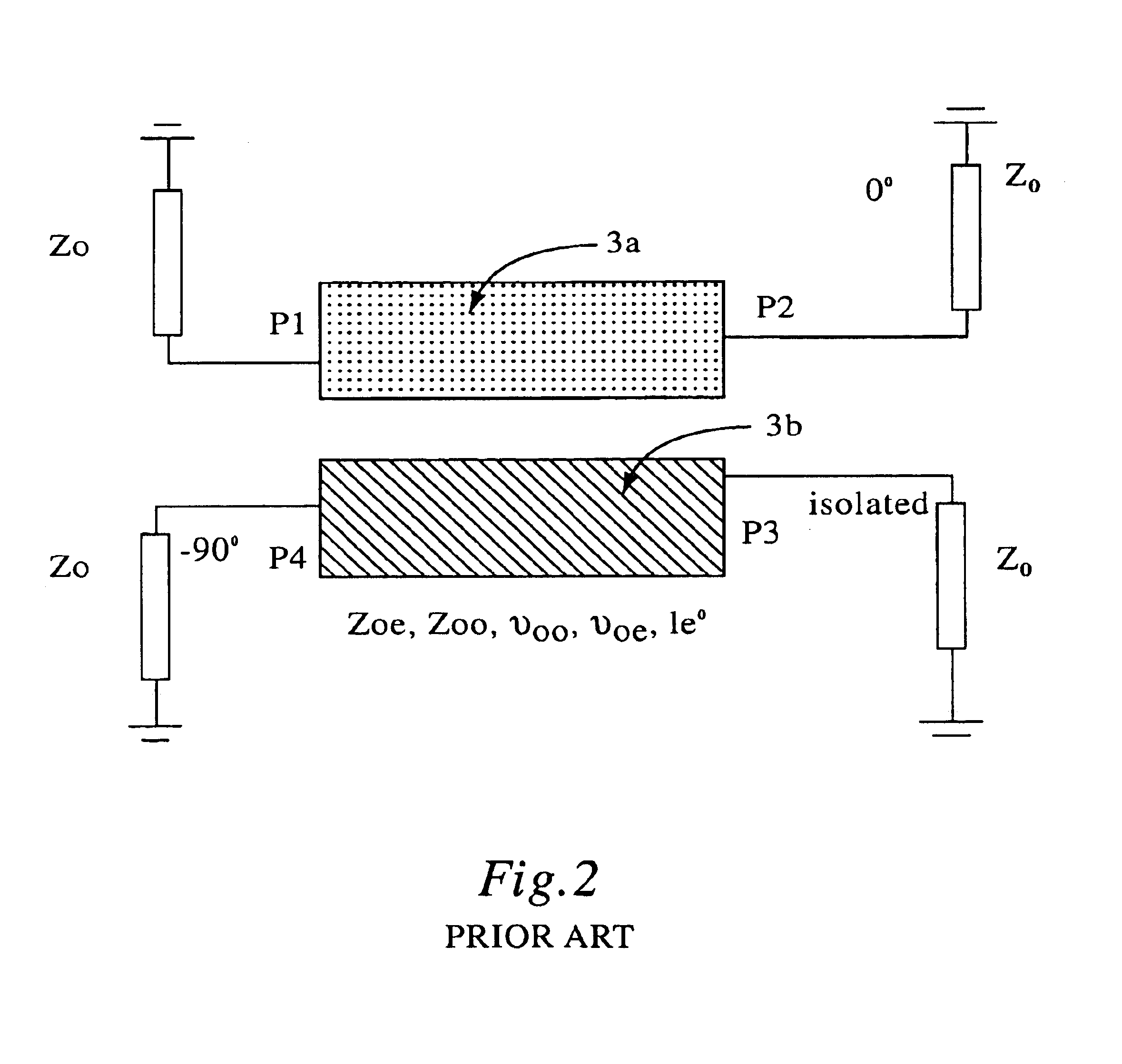
[0073]The homogeneity of the stripline coupler is disturbed by the addition of the short-circuit stub. However, by the use of a principle that may be referred to as “Capacitors-to-Ground”, and described in patent application no. PCT / EP01 / 02249 by the same inventors, one can rectify this problem and preserve overall performance. The disclosure of C this earlier document is incorporated herein by reference.

[0074]In brief, according to this principle, at least one capacitor C1, C2, C3, C4 is connected between a first end of at least one of said at least two lines 3a, 3b and said first conductive layer 2 (for microstrip couplers). In case of stripline couplers, additionally or alternatively, at least one capacitor C1, C2, C3, C4 is connected between a first end of at least one of said at least two lines 3a, 3b and said second conductive layer 2′.

[0075]As regards the capacitors, a respective capacitor C1, C4 is constituted by a conductive member Cp1, Cp4 facing...


PUM


Abstract

Conventional stripline implementations of couplers in Multilayer Ceramic Integrated Circuit (MCIC) technology incur a cost disadvantage when compared to an equivalent microstrip implementation. This is primarily due to the increased substrate thickness needed to achieve the required performance. Conventional stripline couplers significantly limit our ability to optimise for smaller substrate thickness and therefore overall cost. However, stripline couplers are needed for stacked integration scenarios and as building blocks for complex active and passive RF circuits in MCICs. A method of implementation that overcomes this practical disadvantages is therefore highly desirable. To this end, the present invention presents a novel coupling device structure that enable RF designers to use the stripline coupler configuration, by achieving required levels of performance with much reduced substrate thickness. The invention outlines a structured design procedure and presents simulation results confirming the validity of the technique. In particular, to achieve this, the present invention proposes a coupling device, comprising a substrate 1, a first conductive layer 2 covering a first surface of said substrate 1, at least two electromagnetically coupled lines 3a, 3b being provided opposite to said first surface and being covered by at least one cover layer 4, 5, wherein at least one short-circuit stub Stub A, Stub B is connected between at least one of said electromagnetically coupled lines and said first conductive layer.

Description

FIELD OF THE INVENTION[0001]The present invention relates to a coupling device. More particularly, the present invention relates to a coupling device resulting from a multilayer integrated circuit technology fabrication process.BACKGROUND OF THE INVENTION[0002]Coupling devices (referred to as couplers) in general, such as for example Hybrid 3 dB couplers, are essential circuit components which are increasingly being used for high performance applications in such diverse circuits as RF mixers, amplifiers and Modulators. In addition they can be used in a variety of other support functions such as the ones encountered in general RF signal and amplitude Conditioning and error signal retrieval systems.[0003]The expression “hybrid” in connection with couplers means an equal split of power between two (output) ports of the coupler with respect to an input port. Hence a 3 dB coupler is a “hybrid” since:10 log(Powerout / Powerin)=−3 dBPowerout / Powerin=10(−3 / 10)=0.5[0004]So the output power Pow...

Claims


Application Information

Patent Timeline
IPC IPC(8): H01P5/00H03H7/38H01P5/18
CPCH01P5/187H01P5/185
Inventor AL-TAEI, SARMADPASSIOPOULOS, GEORGE
Owner NOKIA CORP
Why Eureka
Try Eureka