Multi-domain liquid crystal display device having a common-auxiliary electrode and dielectric structures
a liquid crystal display device and dielectric structure technology, applied in non-linear optics, instruments, optics, etc., can solve the problem of long time when the liquid crystal director reaches a stable state relatively, and achieve the effect of increasing the time of liquid crystal director stability
- Summary
- Abstract
- Description
- Claims
- Application Information
AI Technical Summary
Benefits of technology
Problems solved by technology
Method used
Image
Examples
first embodiment
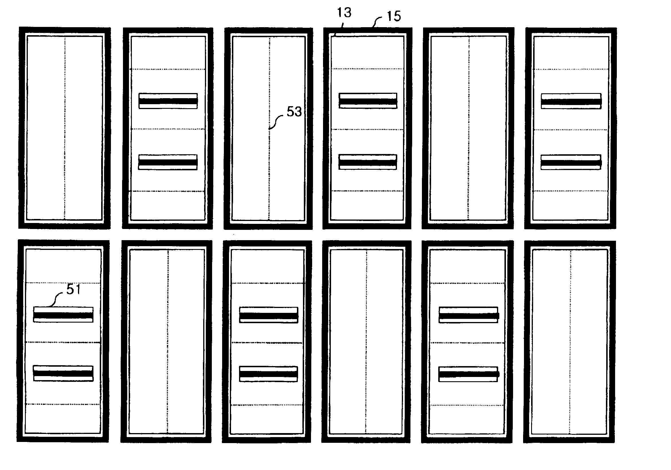
[0057]In the multi-domain liquid crystal display device shown in FIG. 3, the common auxiliary electrode 15 is formed to surround the pixel region. The dielectric structure 53 in one pixel is formed in horizontal direction while the dielectric structure in a neighboring pixel is formed in vertical direction. Moreover, an electric field induction window 51 of a hole or slit is formed in the pixel electrode 13. Thus, the multi-domain liquid crystal display device having an improved characteristic as compared with the first embodiment is obtained.
[0058]Furthermore, in FIGS. 3b and 3d, the passivaiton film 37 is formed of a material such as SiNx or SiOx. In FIGS. 3c and 3e, the passivation film is formed of BCB, acrylic resin or polyimide.
[0059]In the multi-domain liquid crystal display device of FIGS. 3d and 3e, the pixel electrode 13 overlaps the common auxiliary electrode 15 to form a storage capacitor. The light-shielding layer 25 also overlaps the common auxiliary electrode. Accordi...
second embodiment
[0060]In the multi-domain liquid crystal display device shown in FIG. 4, the common auxiliary electrode. 15 is formed to surround the pixel region. The dielectric structure 53 in one pixel is formed in horizontal direction while the dielectric structure in a neighboring pixel is formed in vertical direction. Moreover, two or more electric field induction windows 51 of holes or slits are formed in the pixel electrode 13. Thus, the multi-domain liquid crystal display device of FIG. 4 has an improved characteristic as compared with the
[0061]Furthermore, in FIGS. 4b and 4d, the passivation film 37 is formed of a material such as SiNx, or SiOx. In FIGS. 4c and 4e, the passivation film 37 is formed of BCB, acrylic resin or polyimide.
[0062]In the multi-domain liquid crystal display device of FIGS. 4d and 4e, the pixel electrode 13 overlaps the common auxiliary electrode 15 to form a storage capacitor. The light-shielding layer 25 also overlaps the common auxiliary electrode. Accordingly, a...
fourth embodiment
[0066]In the multi-domain liquid crystal display device shown in FIG. 6, the dielectric structure 53 in one pixel is formed in horizontal direction while the dielectric structure in a neighboring pixel is formed in vertical direction. Moreover, two or more electric field induction windows 51 of holes or slits are formed in the pixel electrode 13. The common auxiliary electrode 15 is formed in a region where the electric field induction windows are formed and around the pixel region. Thus, the multi-domain liquid crystal display device of FIG. 4 has an improved characteristic as compared with the
[0067]Furthermore, in FIGS. 6b and 6d, the passivation film 37 is formed of a material such as SiNx or SiOx, In FIGS. 6c and 6e, the passivation film 37 is formed of BCB, acrylic resin or polyimide.
[0068]In the multi-domain liquid crystal display device of FIGS. 6d and 6e, the pixel electrode 13 overlaps the common auxiliary electrode 15 to form a storage capacitor. The light-shielding layer ...
PUM
| Property | Measurement | Unit |
|---|---|---|
| dielectric constants | aaaaa | aaaaa |
| dielectric constants | aaaaa | aaaaa |
| electric field | aaaaa | aaaaa |
Abstract
Description
Claims
Application Information
 - R&D
- Intellectual Property
- Life Sciences
- Materials
- Tech Scout
- Unparalleled Data Quality
- Higher Quality Content
- 60% Fewer Hallucinations
Browse by: Latest US Patents, China's latest patents, Technical Efficacy Thesaurus, Application Domain, Technology Topic, Popular Technical Reports.
© 2025 PatSnap. All rights reserved.Legal|Privacy policy|Modern Slavery Act Transparency Statement|Sitemap|About US| Contact US: help@patsnap.com


