Voltage generating circuit with two resistor ladders
a voltage generation circuit and resistor ladder technology, applied in pulse generators, instruments, pulse techniques, etc., can solve the problems of consuming considerable power, occupying considerable space, and increasing the number of amplifiers proportionally, so as to reduce overshoot and undershoot
- Summary
- Abstract
- Description
- Claims
- Application Information
AI Technical Summary
Benefits of technology
Problems solved by technology
Method used
Image
Examples
first embodiment
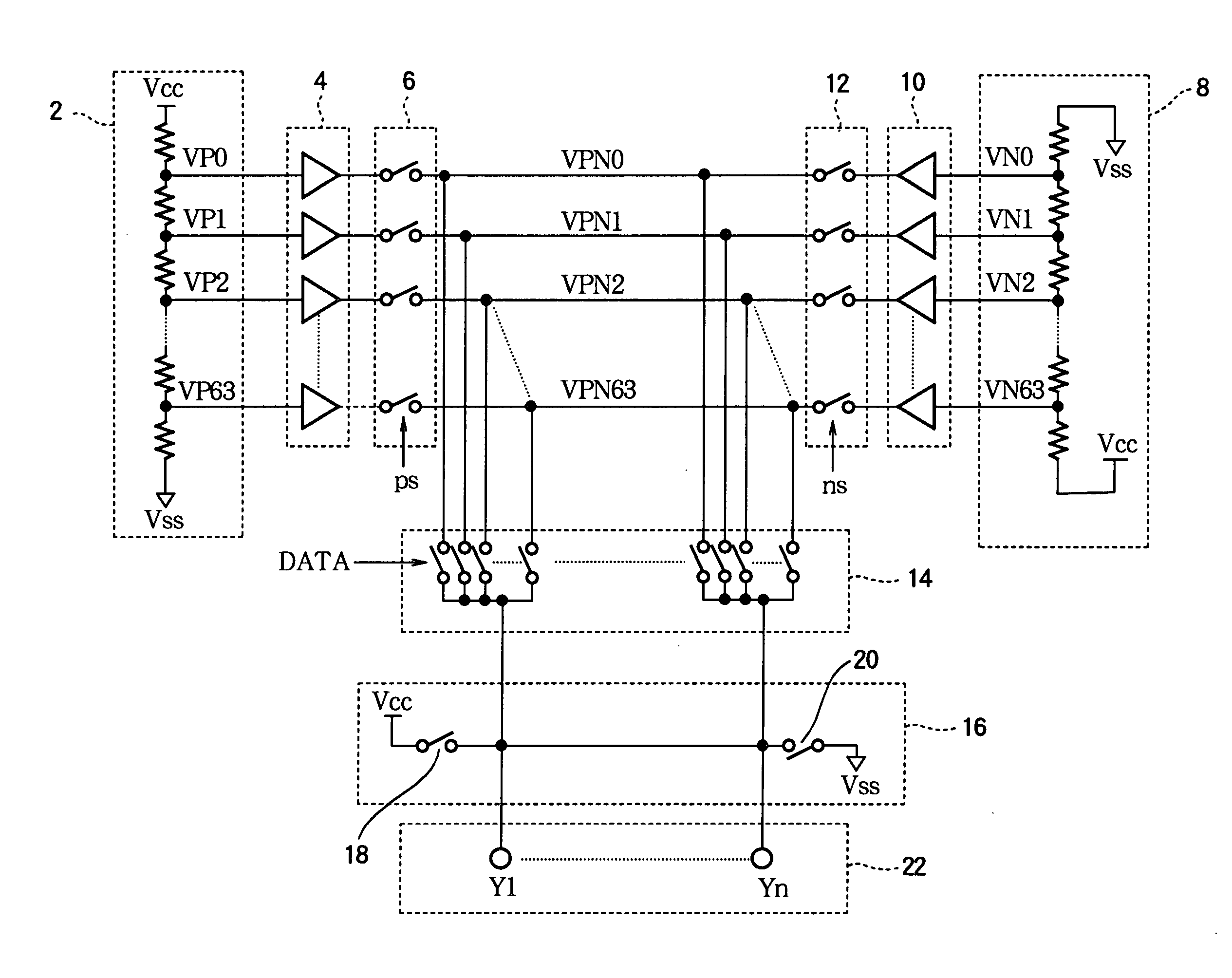
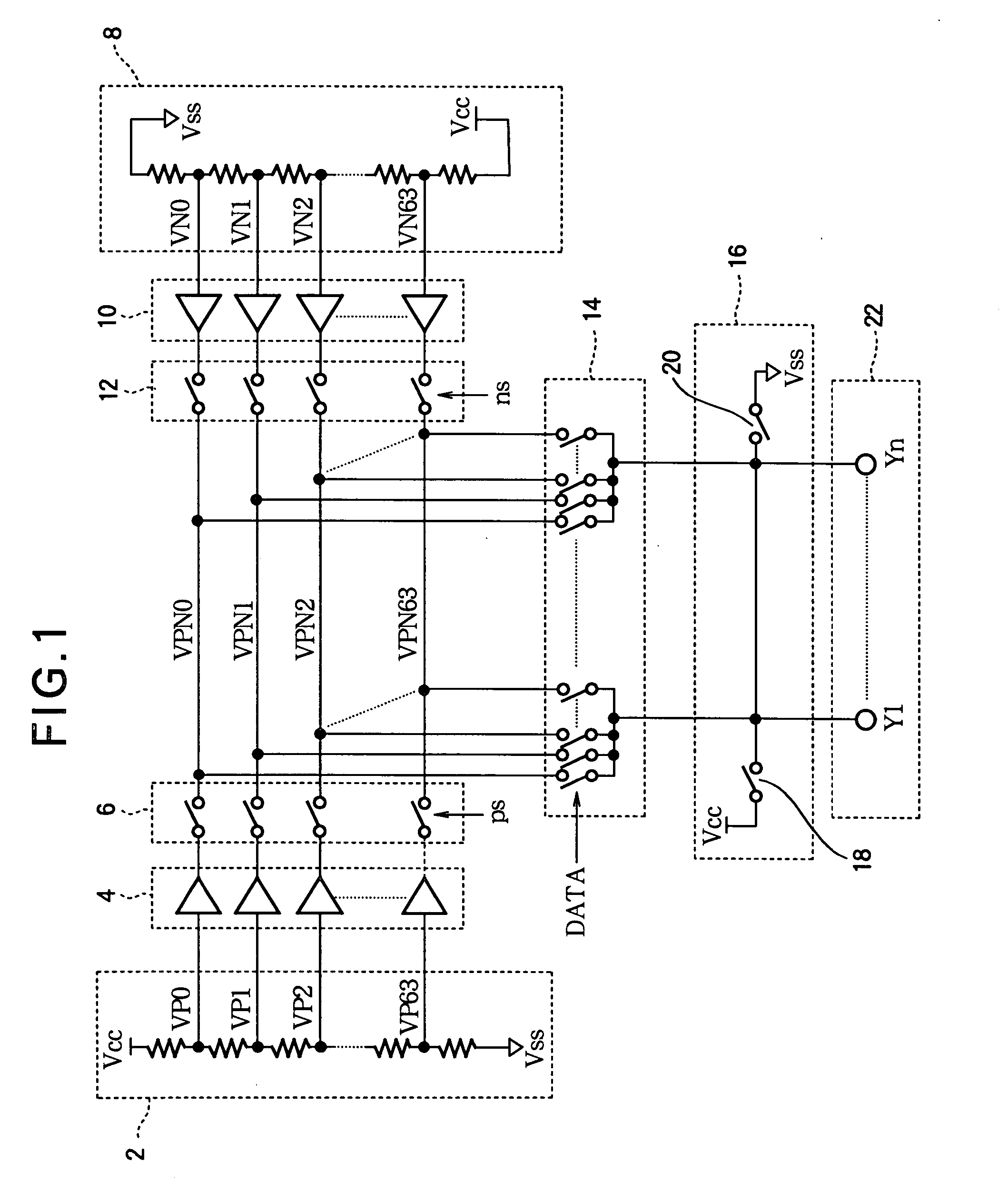
[0035]Referring to FIG. 1, invention is a voltage generating circuit comprising a first resistor ladder 2, a first plurality of amplifiers 4, a first plurality of analog switches 6, a second resistor ladder 8, a second plurality of amplifiers 10, a second plurality of analog switches 12, an output switching circuit 14, a precharging circuit 16 including a pair of switches 18, 20, and a plurality of output terminals 22. In the following description it will be assumed that the output terminals 22, denoted Y1 to Yn, are connected to the source lines of a TFT-LCD panel having a horizontal resolution of n picture elements (pixels), where n is an arbitrary integer greater than one.
[0036]The first resistor ladder 2 receives a first potential Vcc at one end and a second potential Vss at another end, and has sixty-four taps from which voltages VP0 to VP63 intermediate between Vcc and Vss are output. VP0 is relatively close to the Vcc potential, and VP63 is relatively close to the Vss potenti...
second embodiment
[0097]FIG. 16 illustrates the general circuit configuration of the invention. This embodiment eliminates the analog switches in FIG. 1 and connects the amplifiers 4, 10 directly to the internal signal lines VPN0–VPN63.
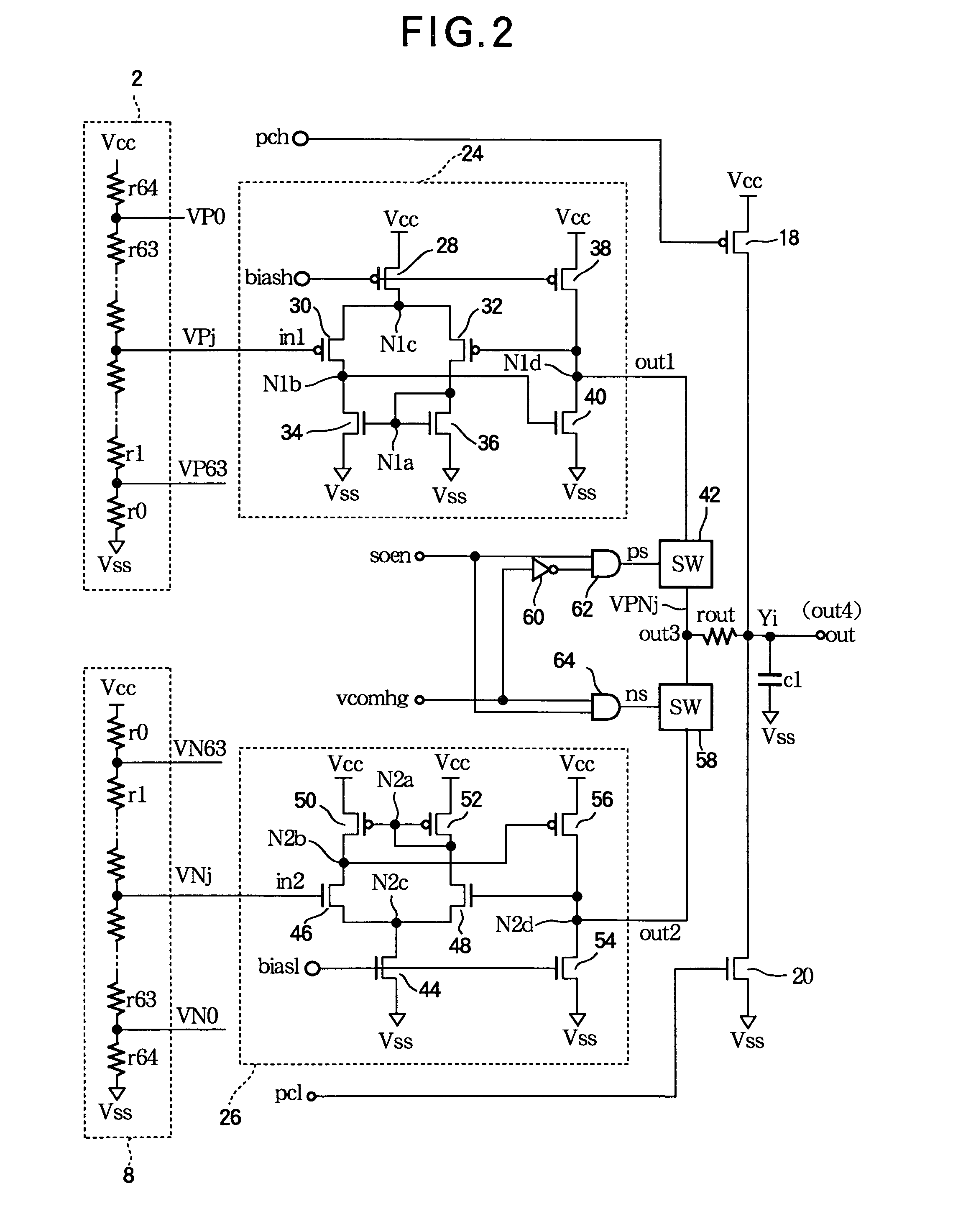
[0098]FIG. 17 illustrates the circuit configuration of the second embodiment in more detail by showing the internal structure of the amplifiers 24, 26 connected to an internal signal line VPNj, where j is an arbitrary integer from 0 to 63. Amplifier 24, which is one of the first plurality of amplifiers 4, combines the features of the first amplifier 24 in FIGS. 12 and 15: that is, it has the basic structure shown in FIG. 2, with additional PMOS transistors 82 and 84 that interrupt current flow during negative driving cycles, and an additional NMOS transistor 76 that turns off NMOS transistor 40 and pulls node N1b down to the Vss level during negative driving cycles. Amplifier 26, which is one of the second plurality of amplifiers 10, similarly combines the features of ...
PUM
 Abstract
Description
Claims
Application Information
 - R&D
- Intellectual Property
- Life Sciences
- Materials
- Tech Scout
- Unparalleled Data Quality
- Higher Quality Content
- 60% Fewer Hallucinations
Browse by: Latest US Patents, China's latest patents, Technical Efficacy Thesaurus, Application Domain, Technology Topic, Popular Technical Reports.
© 2025 PatSnap. All rights reserved.Legal|Privacy policy|Modern Slavery Act Transparency Statement|Sitemap|About US| Contact US: help@patsnap.com


