Light emitting diode with wavelength conversion
- Summary
- Abstract
- Description
- Claims
- Application Information
AI Technical Summary
Benefits of technology
Problems solved by technology
Method used
Image
Examples
Embodiment Construction
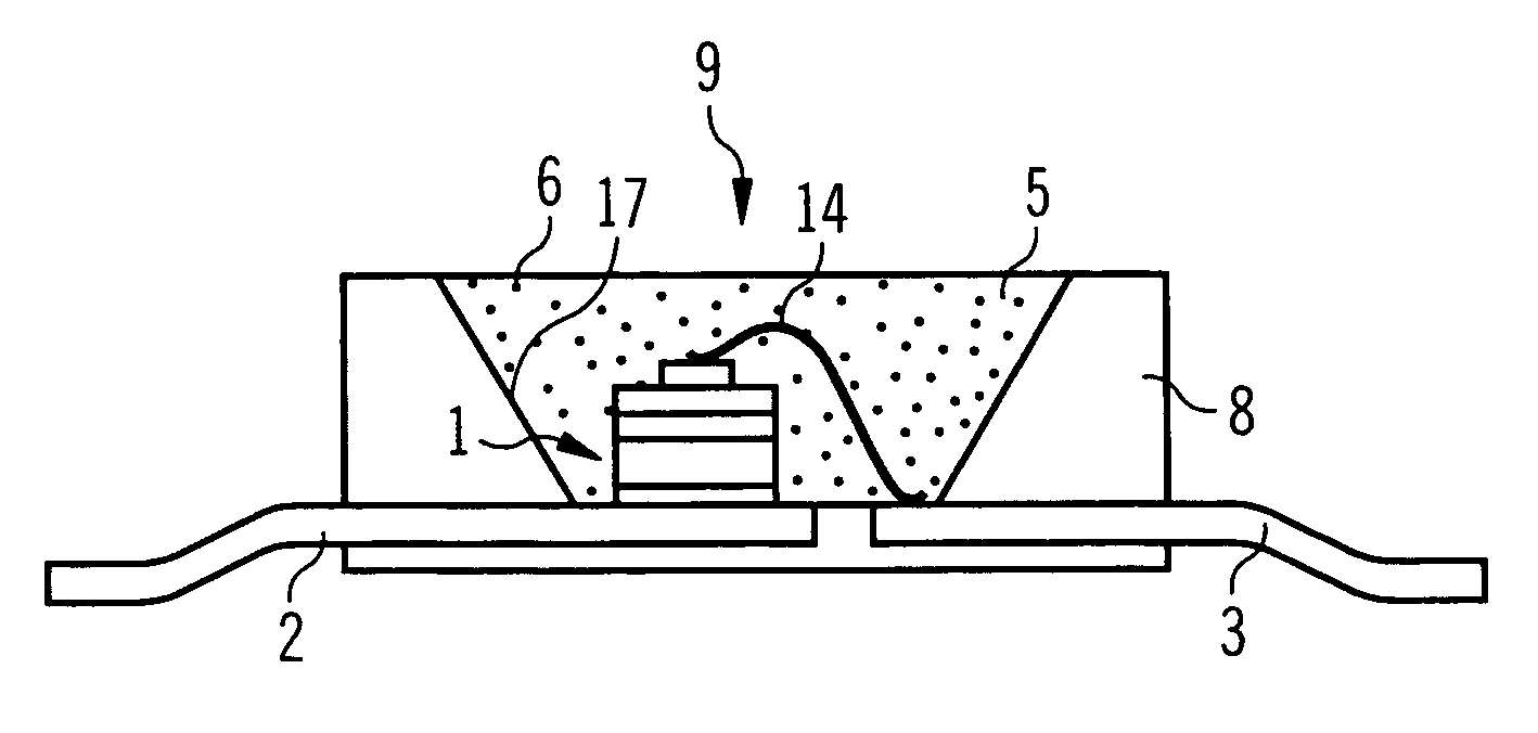
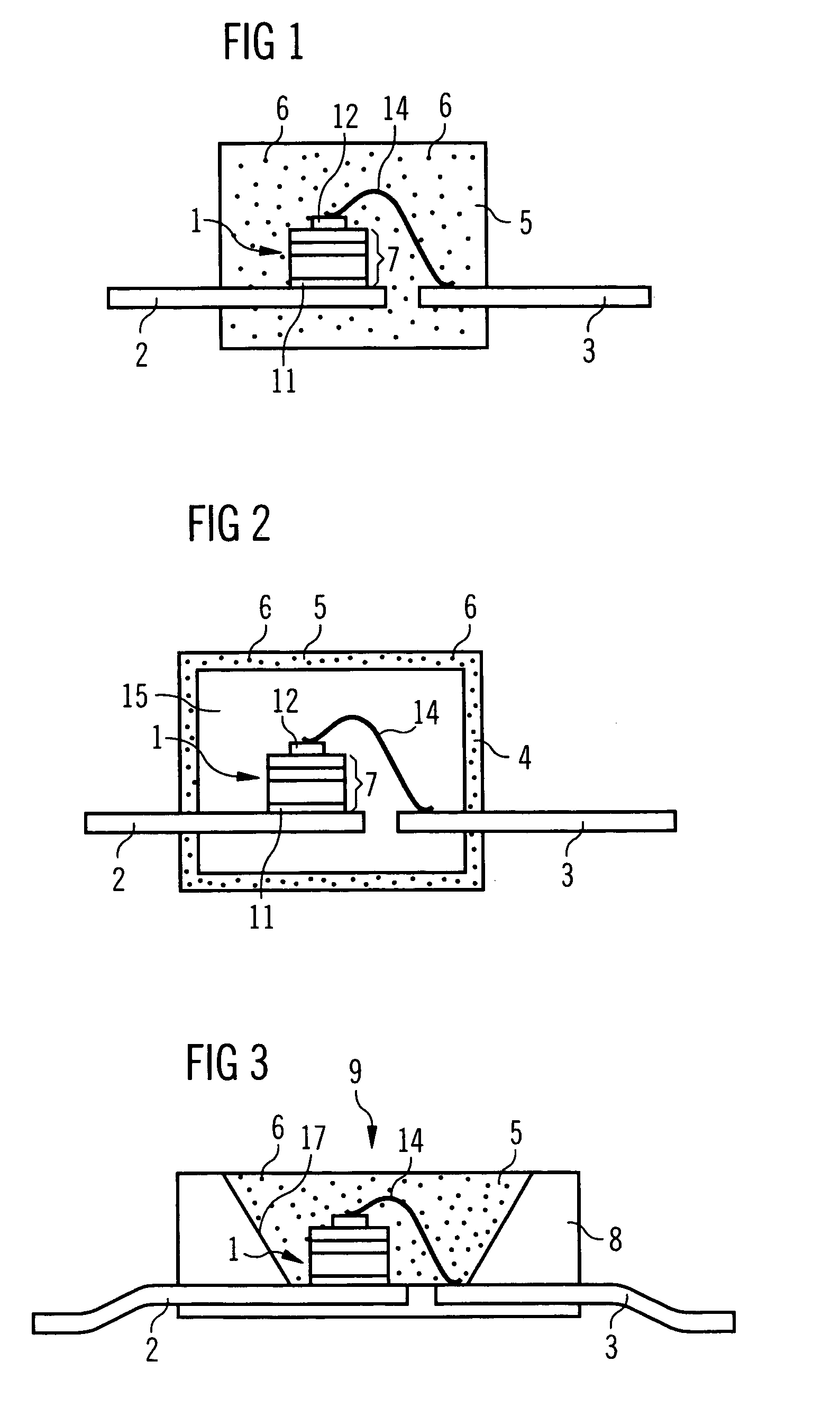
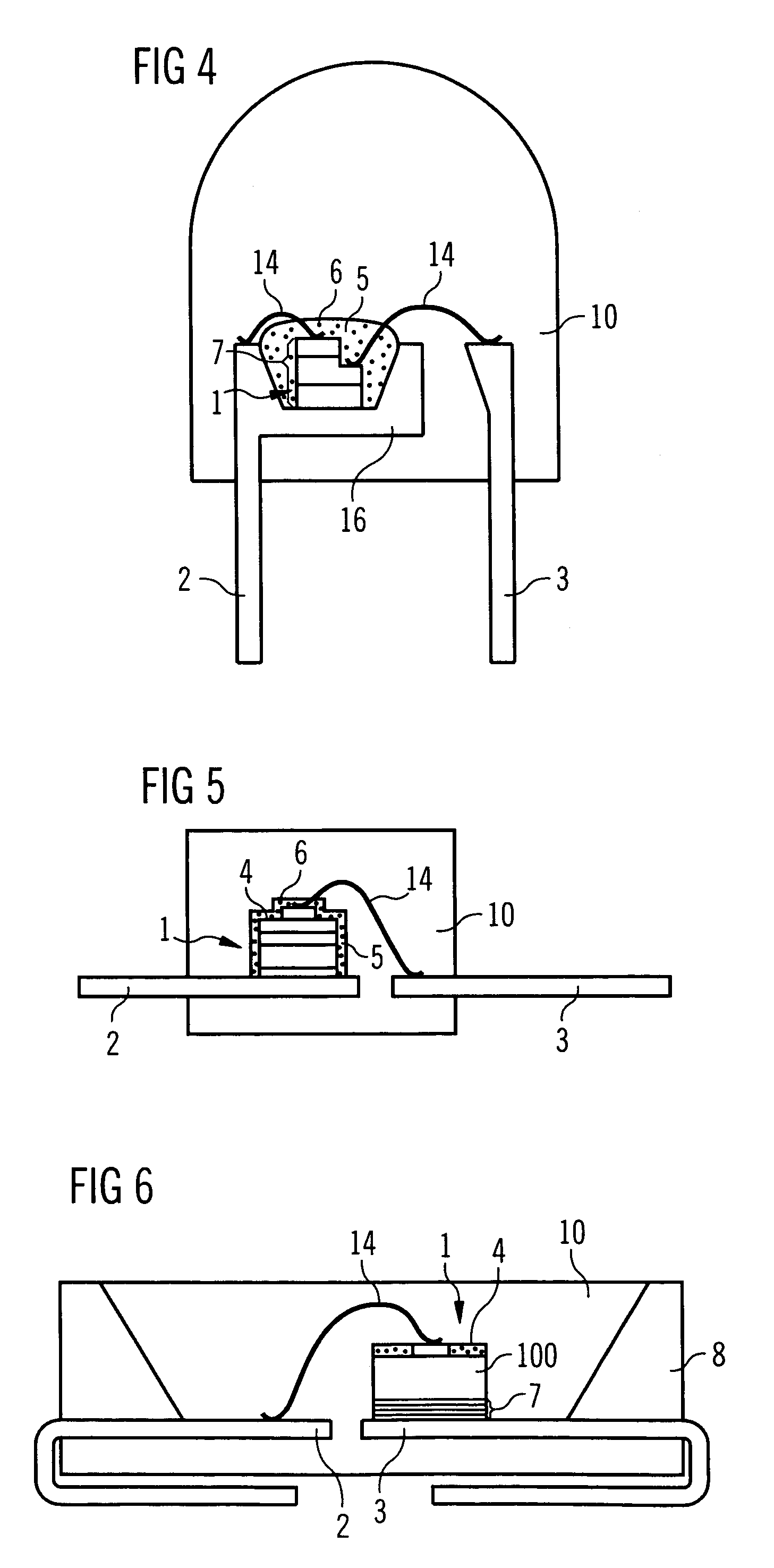
[0063]The light-emitting semiconductor element of FIG. 1 has a reaction resin compound according to the invention. Semiconductor body 1, an LED chip 7 having an active layer or sequence of layers (for example a multi-quantum well structure), having one or a plurality of layers based on InxGayAll-x-yN (where 0≦x≦1, 0≦y≦1 and x+y11 attached to a first electrical connector 2 of a lead frame by means of an electrically conductive connecting element, for example a metallic solder, especially a soft solder, or an adhesive. The front contact 12 is connected to a second electrical connector 3 of the lead frame by means of a bond wire 14.
[0064]The free surfaces of semiconductor body 1 and portions of electrical connectors 2 and 3 are directly enclosed by a hardened, wavelength-converting reaction resin compound 5. Preferably, the latter has epoxy resin, luminescent powder of Ce-doped garnet material (for example YAG:Ce) having a concentration between 1% by weight inclusive and 15% by weight ...
PUM
 Abstract
Description
Claims
Application Information
 - R&D
- Intellectual Property
- Life Sciences
- Materials
- Tech Scout
- Unparalleled Data Quality
- Higher Quality Content
- 60% Fewer Hallucinations
Browse by: Latest US Patents, China's latest patents, Technical Efficacy Thesaurus, Application Domain, Technology Topic, Popular Technical Reports.
© 2025 PatSnap. All rights reserved.Legal|Privacy policy|Modern Slavery Act Transparency Statement|Sitemap|About US| Contact US: help@patsnap.com


