Phase-change optical information recording medium, and optical information recording and reproducing apparatus and method for the same
a technology of optical information and recording medium, which is applied in the direction of optical recording/reproducing/erasing methods, instruments, record information storage, etc., can solve the problems of high noise level in the low power region, especially becoming evident, and achieves improved recording and reproducing properties, low light transmittance, and less errors
- Summary
- Abstract
- Description
- Claims
- Application Information
AI Technical Summary
Benefits of technology
Problems solved by technology
Method used
Image
Examples
example 1
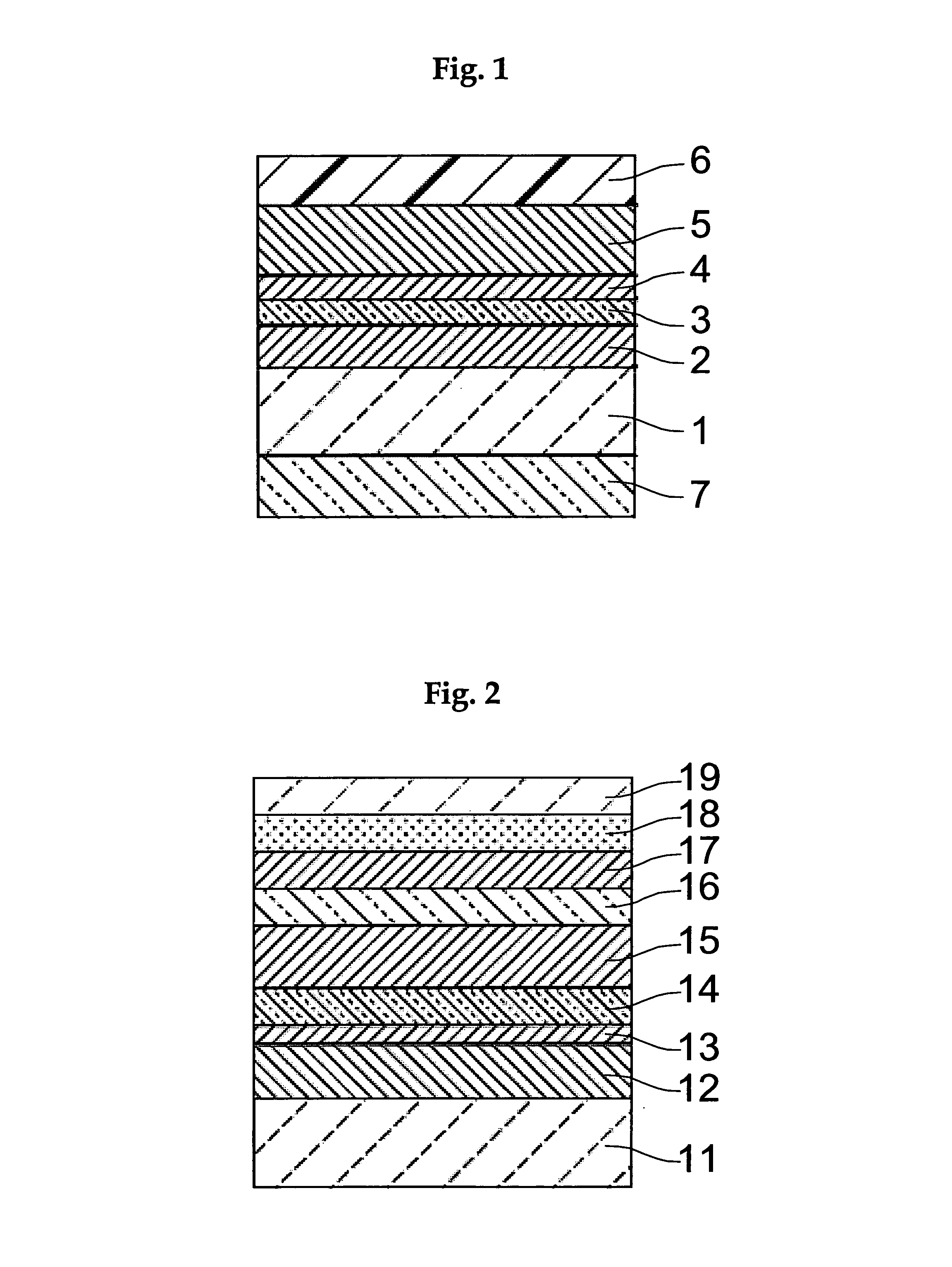
[0044]On a disk-shaped polycarbonate substrate having a track pitch of 0.35 μm, a thickness of 1.1 mm and a diameter of 120 mm, a first protective layer (ZnS—SiO2) having a thickness of 40 nm, a recording layer (Sb68Te29Ge3) having a thickness of 12 nm, a second protective layer (ZnS—SiO2) having a thickness of 14 nm, and a heat-resistant layer (AgPdCu) having a thickness of 120 nm were formed in this order by a sheet fed spatter device. On the obtained structure, radical UV resin (MH7617N, produced by Mitsubishi Rayon Co., Ltd.) was thickened to 5 μm as well as forming a light transmittance thermally controllable layer (Sb2O3) to a 30 nm-thick at a side of the disk where a light beam transmits. Thus, a phase-change optical disk having a final thickness of 1.2 mm according to the present invention was formed as shown in FIG. 1.
examples 2 – 4
Examples 2–4
[0054]Phase-change optical disks according to the present invention were prepared following the same procedure as in Example 1, except for using material described in Table 1 as the light transmittance thermally controllable layer. The recording layers of the prepared phase-change optical disks were initialized and examined for their reproducing qualities as in Example 1. The results are shown in Table 1.
examples 5 – 8
Examples 5–8
[0055]On a disk-shaped polycarbonate substrate having a track pitch of 0.35 μm, a thickness of 1.1 mm and a diameter of 120 mm, a heat-resistant layer (Ag94Cu3Pd3) having a thickness of 100 nm, a third protective layer (ZnS—SiO2) having a thickness of 3 nm, a light transmittance thermally controllable layer (Table 1), a second protective layer (ZnS—SiO2) having a thickness of 5 nm, a recording layer (Ag5In5Sb65Te25) having a thickness of 10 nm, and a first protective layer (ZnS—SiO2) having a thickness of 100 nm were formed in this order by a sheet fed spatter machine. On the obtained structure, a thin substrate of polycarbonate having a thickness of 0.6 mm was attached by means of an acrylic adhesive (DA8310-A50, produced by Nitto Denko Corporation). Thus, a phase-change optical disk having a final thickness of 1.2 mm according to the present invention was formed as shown in FIG. 2.
[0056]For crystallization of a recording layer of the phase-change optical disk prepared ...
PUM
| Property | Measurement | Unit |
|---|---|---|
| recording wavelength | aaaaa | aaaaa |
| refractive index | aaaaa | aaaaa |
| thickness | aaaaa | aaaaa |
Abstract
Description
Claims
Application Information
 - R&D
- Intellectual Property
- Life Sciences
- Materials
- Tech Scout
- Unparalleled Data Quality
- Higher Quality Content
- 60% Fewer Hallucinations
Browse by: Latest US Patents, China's latest patents, Technical Efficacy Thesaurus, Application Domain, Technology Topic, Popular Technical Reports.
© 2025 PatSnap. All rights reserved.Legal|Privacy policy|Modern Slavery Act Transparency Statement|Sitemap|About US| Contact US: help@patsnap.com


