
Method of developing a resist film and a resist development processor

a technology of resist film and development processor, which is applied in the field of developing a resist film and a development processor, can solve the problems of inability to prevent the collapse of the pattern, fluctuations in the development, and failure to obtain satisfactory, so as to achieve the effect of precise control of the solubility

Inactive Publication Date: 2006-04-25
HITACHI SCI SYST LTD
View PDF8 Cites 5 Cited by
  • Summary
  • Abstract
  • Description
  • Claims
  • Application Information

AI Technical Summary

Benefits of technology

[0020]An object of the present invention is to provide a method of developing a resist film, a method of treating a surface of a resist film carried on a substrate such as silicon wafer, a resist development processor, and a surface processor that permits microscopic development of the resist film in a short period of time with the minimum fluctuation and maximum accuracy, using such a supercritical fluid as carbon dioxide that eliminates the need of utilizing a chemical solution and a waste liquid treatment facility.
[0021]The present inventors have found out an apparatus and the method for utilizing the same that ensures quick development of an exposed resist film with a supercritical fluid in the aforementioned process, using supercritical carbon dioxide, so as to eliminate the possibility of pattern collapse or the need of using a chemical developer or rinser. The aforementioned apparatus and method can carry out a pattern forming process by removing the photo-exposed resist film or the non photo-exposed portion in the phase of development.
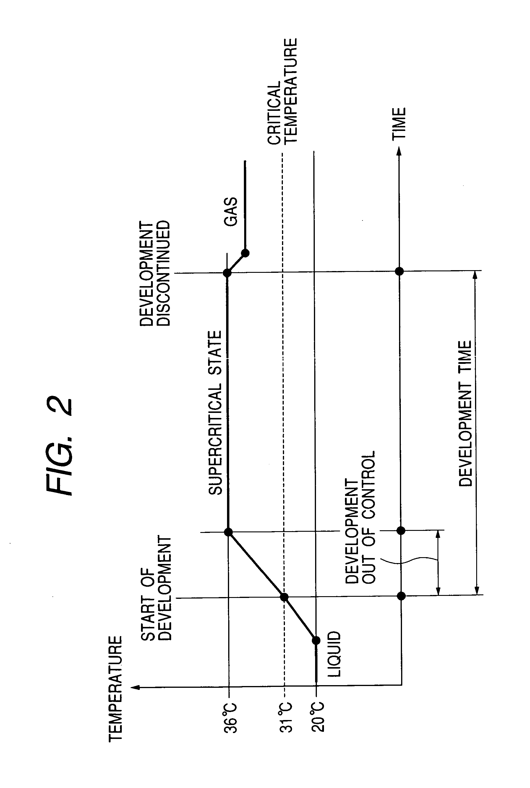
[0022]Dissolution power of the solvent for a solute depends on the temperature and density of the solvent. When a solvent is used as a developer of the resist film, the solvent as a developer may be beyond the critical point, i.e. the supercritical state under the condition for getting dissolution power suitable for developing the resist film. The density of the supercritical fluid can be changed by controlling its pressure and temperature; as a result, its dissolution power can be controlled freely.
[0029]The solubility of carbon dioxide with respect to fluorine-containing polymeric material is about the same as that of hexane. Especially when developing a plurality of large-diameter resist substrates having a diameter of 200 mm or more, a large quantity of supercritical carbon dioxide is required. The high pressure container serving as a development processing chamber is required to have a sufficient volume to accommodate the amount of supercritical carbon dioxide needed for development. This leads to an increase in the size of the development processing chamber and heat capacity.
[0044]a temperature regulator for regulating so as to minimize the difference in the temperatures of the aforementioned development solvents supplied into the aforementioned development processing chamber from each container.
[0071]The resist development apparatus and the method thereof, using supercritical fluid according to the present invention, ensures precise control of the solubility of a supercritical fluid as a development solvent. In the formation of a minute pattern having a resist width of 100 nm through 20 nm (for future), this invention permits development of the resist pattern without variation where high-performance characteristics are required. Alternatively, the surface processor and the method thereof allow quick processing in the phase of cleaning and drying, separately from the aforementioned development, and are capable of meeting the requirements in minute pattern formation.

Problems solved by technology

The prior art method cannot prevent the pattern from collapse.
This leads to the failure to obtaining a satisfactory result.
This results in phenomena that are beyond the control, thereby causing fluctuations in development.

Method used


Image

  • Method of developing a resist film and a resist development processor
  • Method of developing a resist film and a resist development processor
  • Method of developing a resist film and a resist development processor

Examples


Embodiment Construction

Description of the Preferred Embodiments

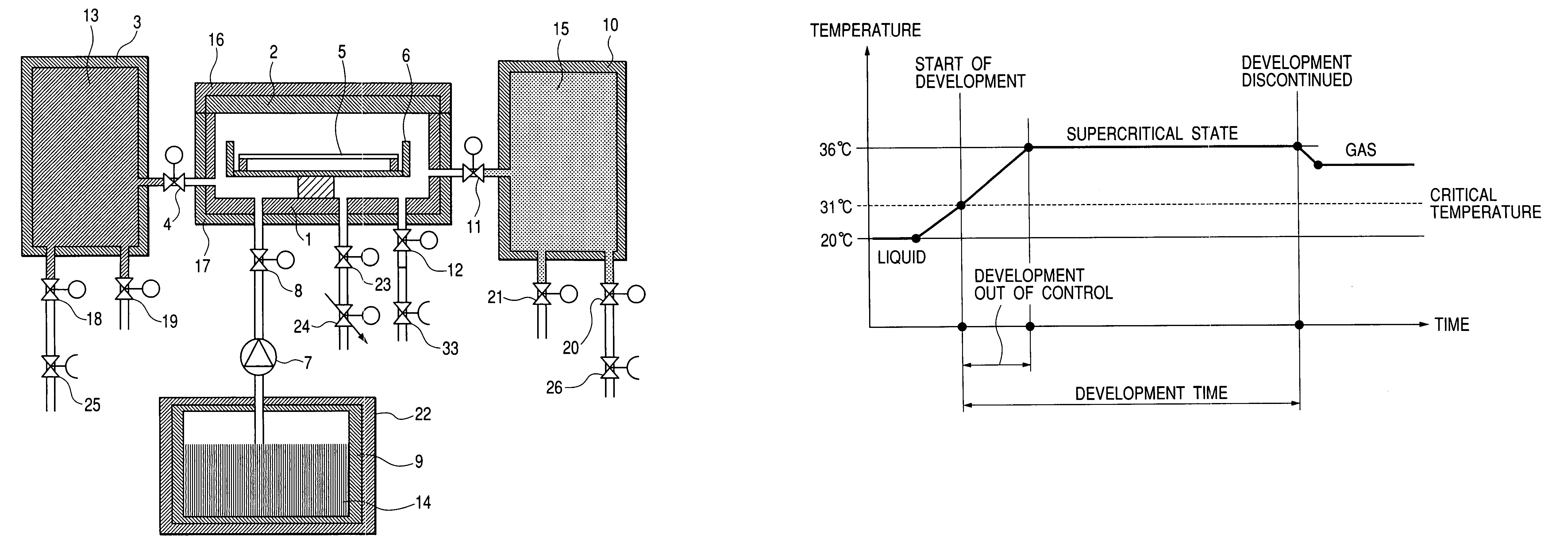
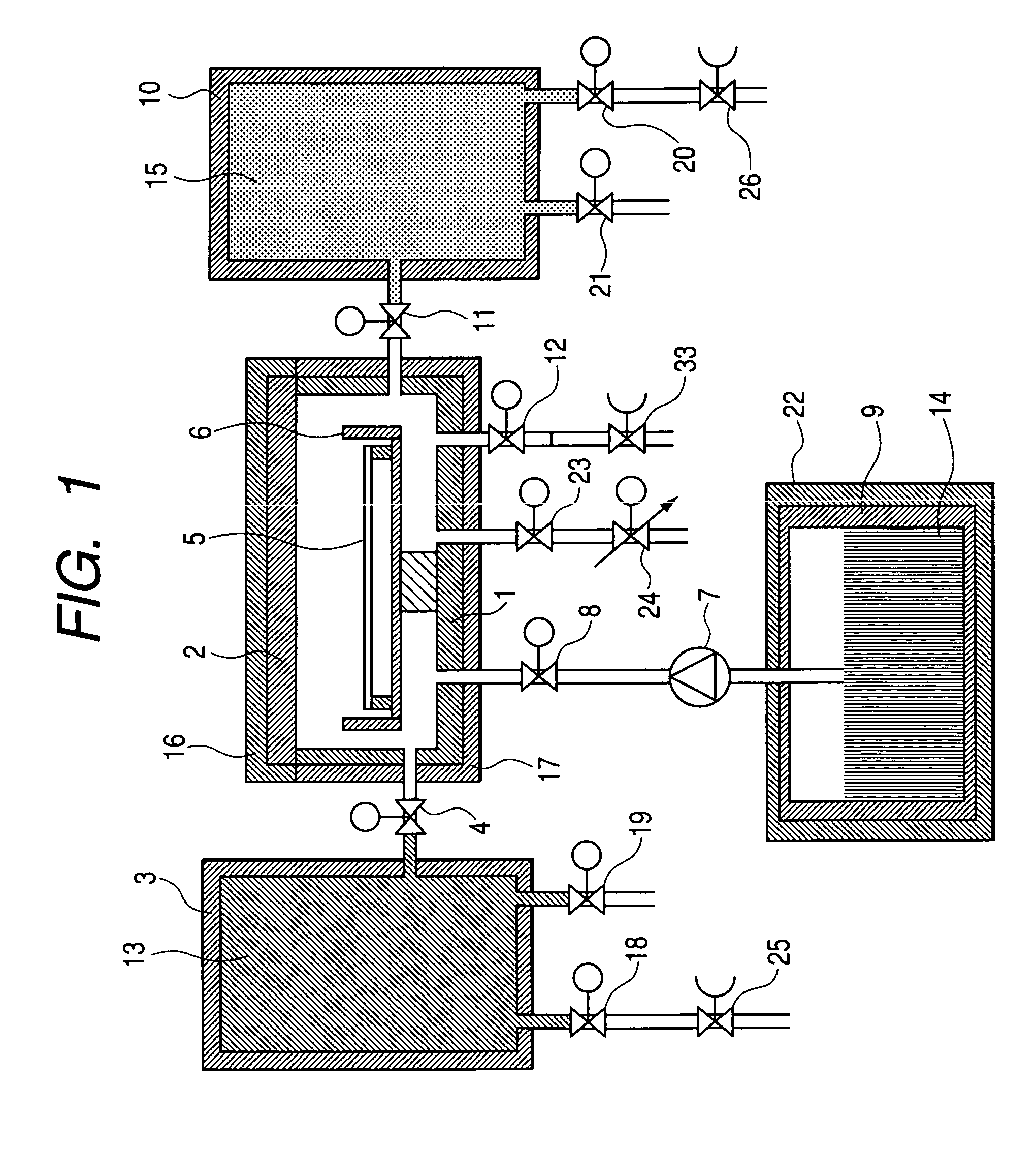
[0079]FIG. 1 is a block diagram representing a supercritical resist development apparatus according to the present invention. A supercritical carbon dioxide container 3 filled with supercritical carbon dioxide 13 at a pressure of 20 MPa and a temperature of 40 degrees Celsius is connected through a valve 4 to the development processing chamber 1 controlled to have a temperature of 30 degrees Celsius. After a resist substrate 5 coated with exposed fluorine-containing polymeric material has been installed in the substrate holder 6 inside the development processing chamber 1, the development processing chamber 1 is enclosed with a cover 2. The valves 4, 8, 11, 12 and 23 connected to the development processing chamber 1 are closed and a valve 20 connected to the high pressure carbon dioxide gas container 10 is opened.

[0080]When the siphon-based liquid carbon dioxide container 9 is controlled to 25 degrees Celsius by the temperature regulator 22, t...


PUM

PropertyMeasurementUnit
diameteraaaaaaaaaa
critical pressureaaaaaaaaaa
critical temperatureaaaaaaaaaa

Abstract

The present invention provides a resist development processor consisting of a development processing chamber for storing a resist substrate having an exposed resist on the substrate and for developing the exposed resist by means of a development solvent consisting of a supercritical fluid; and a supercritical fluid container for storing a supercritical fluid, where the supercritical fluid container is connected to the development processing chamber through a valve.

Description

BACKGROUND OF THE INVENTION[0001]1. Field of the Invention[0002]The present invention relates to a method of developing a resist film formed on a substrate such as an LSI, a method of surface treatment of the resist film, a development processor for the resist, and a surface processor.[0003]2. Related Art[0004]The following publications show related art of the present invention.[0005](1) Patent Document 1; Japanese Patent Laid-Open Publication No. 07-284739 (1995)[0006](2) Patent Document 2; Japanese Patent Laid-Open Publication No. 09-139374 (1997).[0007](3) Patent Document 3; Japanese Patent Laid-Open Publication No. 11-87306 (1999)[0008](4) Patent Document 4; Japanese Patent Laid-Open Publication No. 2001-220828[0009]In manufacturing a large-scale, high-integration density and high-performance device, a resist film, which is formed on a silicon wafer is exposed, developed, rinsed and dried to form a pattern thereon. Then, a process comprising steps of etching the silicon through ...

Claims


Application Information

Patent Timeline
Patent Type & Authority Patents(United States)
IPC IPC(8): G03D5/00G03D3/00G03F7/30G03F7/32H01L21/027
CPCG03D3/00
Inventor TAKASU, HISAYUKIMIYAZAWA, KOUICHIIWAYA, TORU
Owner HITACHI SCI SYST LTD
Learn More