
Leak detection method and micro-machined device assembly

a micro-machined device and leak detection technology, applied in the direction of magnets of measurement instruments, instruments, and semiconductor/solid-state device details, can solve the problem and achieve the effect of measurable instability in diodes over a longer period of tim

Active Publication Date: 2006-04-11
GOOGLE LLC
View PDF12 Cites 3 Cited by
  • Summary
  • Abstract
  • Description
  • Claims
  • Application Information

AI Technical Summary

Benefits of technology

This approach ensures reliable detection of unsealed devices by maintaining measurable humidity levels, reducing the time constraints between soaking and testing, and enhancing the scalability and efficiency of leak detection in manufacturing processes.

Problems solved by technology

The method affects an increase in the time for sufficient water vapor to remain within a leaky or unsealed device, so that instability in the diode can be measurable over a longer period of time.

Method used


Image

  • Leak detection method and micro-machined device assembly
  • Leak detection method and micro-machined device assembly
  • Leak detection method and micro-machined device assembly

Examples


Embodiment Construction

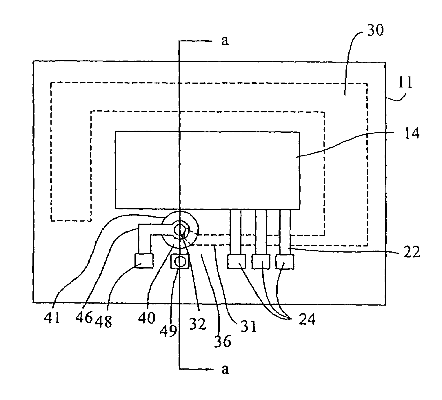
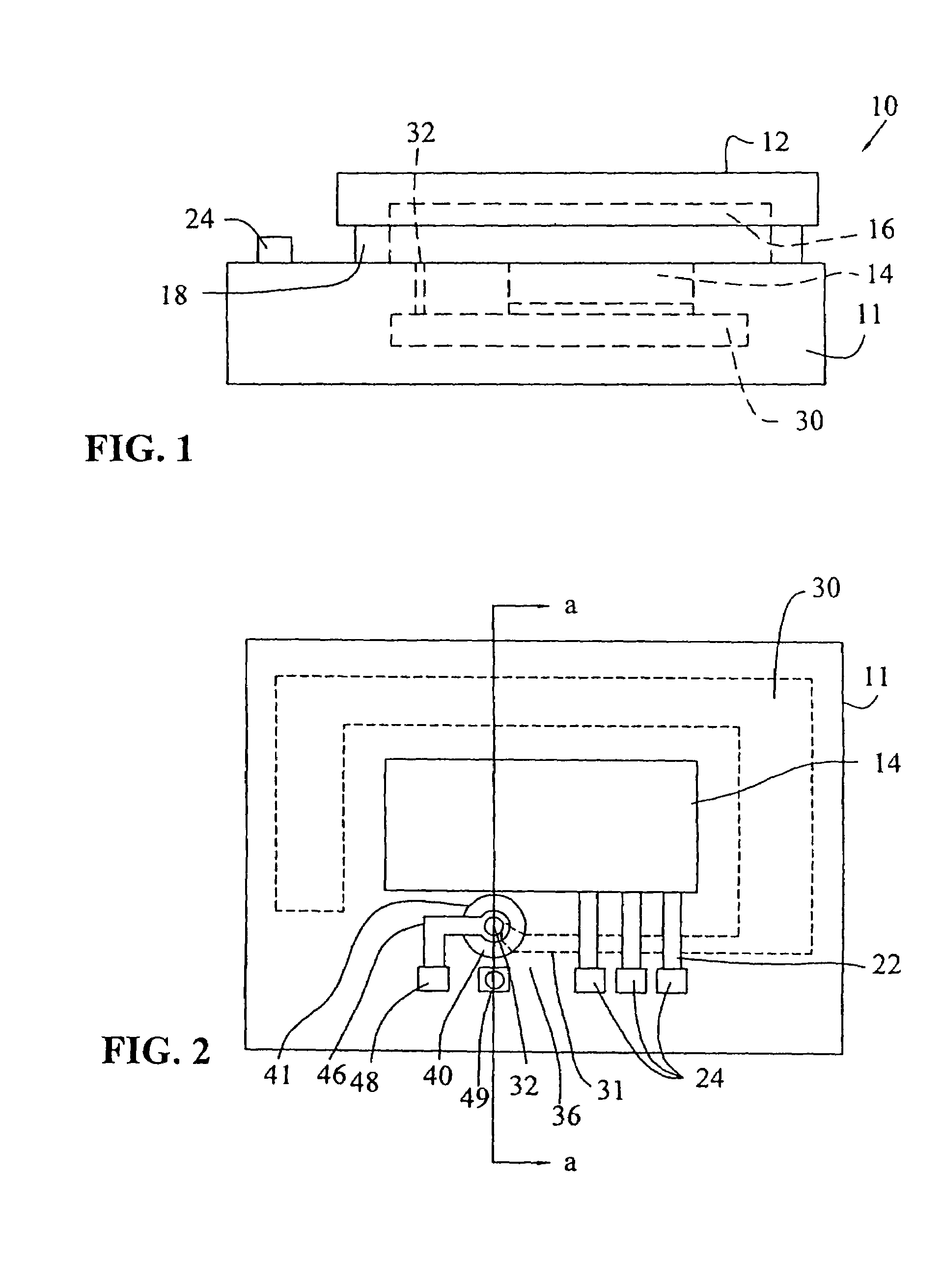
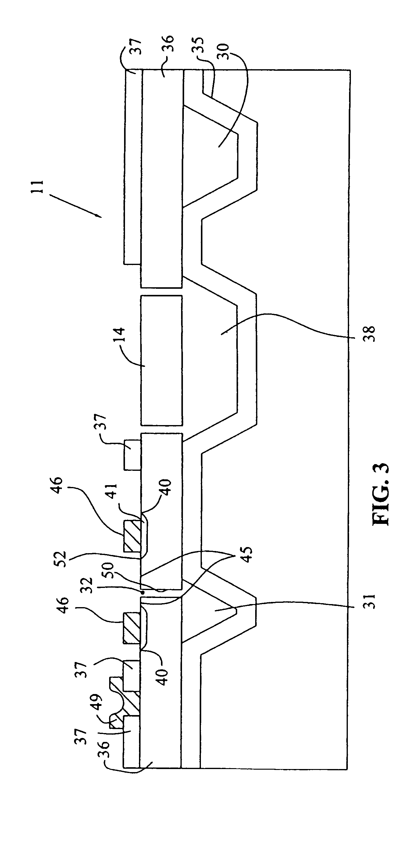
[0025]The method of the present invention employs a reverse current to flow through an exposed, unpassivated, PN junction diode in a semiconductor substrate, and a determination of an instable reverse current, similar to that described in U.S. Pat. No. 6,074,891, herein fully incorporated by reference. The method is based on the discovery that when wet or when exposed to an environment that has a relative humidity greater than about 50%, the unpassivated junction diode characteristics show measurable instability. Once dry, however, the junction diode's characteristics return to normal, and dry but leaky devices are not detected. The method of the present invention assures measurable humidity levels remaining in the cavity so that the junction diode can electrically identify leaky devices.

[0026]FIG. 1 represents a semiconductor sensor or a micro-machined device in accordance with this invention. Device 10 in FIG. 1 is formed by bonding device wafer 11 to capping wafer 12, such that s...


PUM


Abstract

The present invention involves an electrical verification method that detects moisture within the cavity of the semiconductor or micro-machined device. The method affects an increase in the time for sufficient water vapor to remain within an unsealed device, so that instability in the diode can be measurable over a longer period of time. The method begins with the step of forming at least one reservoir on at least one of the device wafer and the capping wafer. The at least one reservoir connects to at least one diffusion channel, which is in communication with at least one reservoir port. The method further includes the steps of forming a PN junction diode adjacent to the at least one reservoir port; bonding the device wafer with the capping wafer to form a cavity; and electrically testing the PN junction diode as an indication of the presence of moisture within the cavity. The device assembly of the present invention includes a capping wafer bonded on a device wafer to form a cavity; at least one reservoir including at least one diffusion channel for receiving a liquid and retaining moisture. The at least one diffusion channel communicates with at least one reservoir port, which is open into the cavity. An exposed PN junction diode is provided adjacent to the at least one reservoir port, and a pair of metal pads is connected to the exposed PN junction diode.

Description

TECHNICAL BACKGROUND[0001]1. Field of the Invention[0002]The present invention relates to a method for detecting leaks in a cavity such as that between semiconductor wafers. More particularly, this invention relates to an electrical verification technique and device for detecting a leak within a cavity enclosing a micro-machined sensing structure.[0003]2. Description of the Related Art[0004]Many micro-electrical-mechanical systems (MEMS) devices such as yaw (angular rate) sensors, accelerometers and pressure sensors employ multiple substrates joined together into a functional stack. For instance, micro-sensor devices that are formed in silicon substrates (referred to herein as a device wafer) are often protected from moisture and particulates by bonding a cap (referred to as capping wafer) to the top surface of the sensor. When the bond is not complete and there is a leak path into the interior of the device stack, moisture and particulates can make their way through the void. Parti...

Claims


Application Information

Patent Timeline
Patent Type & Authority Patents(United States)
IPC IPC(8): H01L29/40H01L29/88G01M3/18G01M3/22G01M3/40
CPCG01M3/186G01M3/40G01M3/226
Inventor CHRISTENSON, JOHN C.RICH, DAVID B.
Owner GOOGLE LLC
Learn More