Color filter substrate and fabricating method thereof
a technology of color filter substrate and substrate, which is applied in the direction of originals for photomechanical treatment, instruments, optical elements, etc., can solve the problems of peeling or cracking of color filter patterns, and achieve the effect of increasing the contact area and enhancing the adhesion between the color filter pattern and the substrate within the sub-pixel region
- Summary
- Abstract
- Description
- Claims
- Application Information
AI Technical Summary
Benefits of technology
Problems solved by technology
Method used
Image

Examples
first embodiment
The First Embodiment
[0020]Reference will now be made in detail to the present preferred embodiments of the invention, examples of which are illustrated in the accompanying drawings. Wherever possible, the same reference numbers are used in the drawings and the description to refer to the same or like parts.
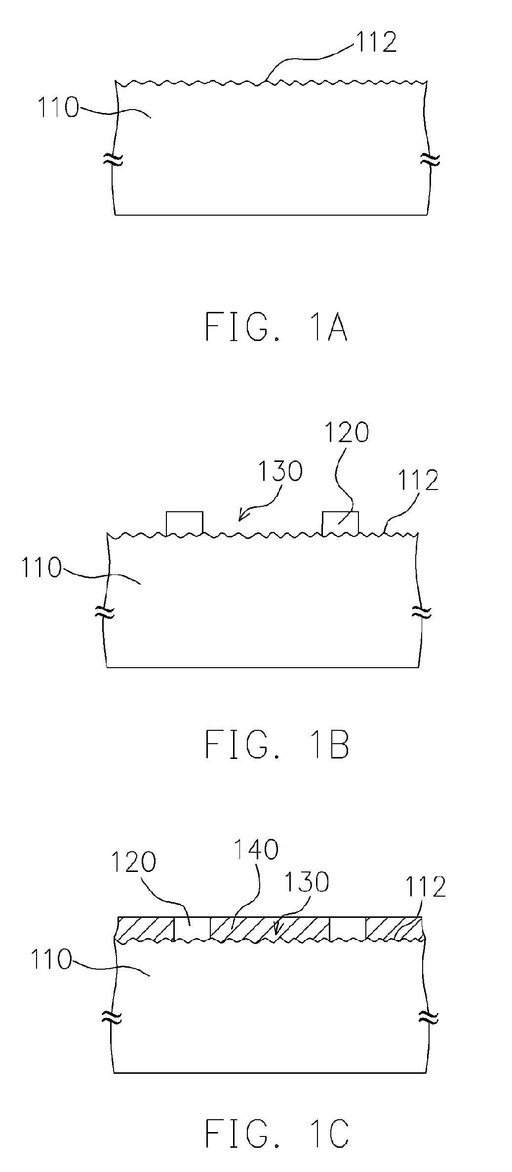
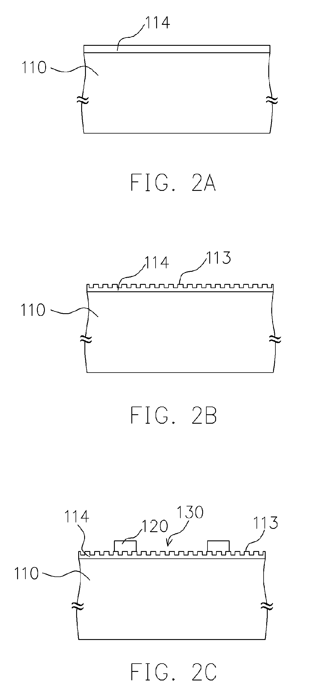
[0021]FIGS. 1A, 1B and 1C are schematic cross-sectional views showing the steps of fabricating a color filter substrate according to one embodiment of the present invention. With reference to FIG. 1A, the fabricating method starts by providing a substrate 110 and performing a roughening process on the substrate 110 to make a rough surface 112 on the substrate 110. In an embodiment, the roughening process described above can be a laser process or an etching process.
[0022]In FIG. 1B, a black matrix 120 is formed on the substrate 110 to define a plurality of sub-pixel regions 130 on the rough surface 120. In one embodiment, the material of the black matrix 120 can be resin or metal. ...
second embodiment
The Second Embodiment
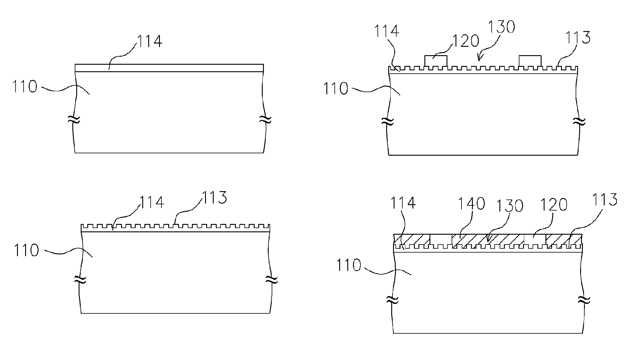
[0028]FIGS. 3A, 3B and 3C are schematic cross-sectional views showing the steps of fabricating a color filter substrate according to still another embodiment of the present invention. As shown in FIG. 3A, the other fabricating method of color filter substrate in the present invention start by forming a black matrix 120 on the substrate 110 of the color filter substrate to define a plurality of sub-pixel regions 130 thereon. The forming method of the black matrix 120 is similar to the method described above.
[0029]Afterwards, as shown in FIG. 3B, a roughening process is performed on the substrate 110 within the sub-pixel regions 130, such that the buffer layer 114 has a rough surface 113. In one embodiment, the roughening process described above can be a laser process or an etching process.
[0030]Finally, as shown in FIG. 3C, a plurality of color filter patterns 140 are formed in the sub-pixel regions 130. Wherein, the forming method of the color filter patterns 14...
PUM
| Property | Measurement | Unit |
|---|---|---|
| diameter | aaaaa | aaaaa |
| surface energy | aaaaa | aaaaa |
| adhesive reliability | aaaaa | aaaaa |
Abstract
Description
Claims
Application Information
 - R&D
- Intellectual Property
- Life Sciences
- Materials
- Tech Scout
- Unparalleled Data Quality
- Higher Quality Content
- 60% Fewer Hallucinations
Browse by: Latest US Patents, China's latest patents, Technical Efficacy Thesaurus, Application Domain, Technology Topic, Popular Technical Reports.
© 2025 PatSnap. All rights reserved.Legal|Privacy policy|Modern Slavery Act Transparency Statement|Sitemap|About US| Contact US: help@patsnap.com