
Method and device for detecting and processing signal waves

a signal wave and signal processing technology, applied in the direction of amplitude demodulation, optical radiation measurement, instruments, etc., can solve the problems of insufficient flow direction of photocharge, high cost of associated receiving apparatus, and insufficient modulation of electrical drift field, etc., to achieve low cost, reduce size, and improve performance and functionality

Inactive Publication Date: 2006-03-14
SCHWARTE RUDOLF
View PDF5 Cites 43 Cited by
  • Summary
  • Abstract
  • Description
  • Claims
  • Application Information

AI Technical Summary

Benefits of technology

[0006]Such a process is intended to enable the receiving apparatuses for the very different properties of the types of signal waves named to be simplified and reduced in size in targeted manner so that at low cost a plurality of receiving pixels can be operated in parallel, performance and functionality increased and e.g. a 3D image can be produced. The receiving apparatus is intended to be designed such that an amplification and processing of the carrier signal is decisively reduced and the performance features such as measurement sensitivity, measurement accuracy etc. are increased.

Problems solved by technology

The associated receiving apparatus is very expensive and generally only contains one receiver.
In spite of this exceptional progress, such PMD pixel receivers have disadvantages: The modulating photogates cause an attenuation of the incident light.
Moreover, the modulating electrical drift field is not optimally introduced into the flow direction of the photocharge.
Furthermore, an essential sensitivity increase by corresponding design of these known CMOS modulation photogate PMDs using a charge carrier multiplication by impact ionization (avalanche effect) or other secondary electron multiplication is scarcely realizable.

Method used


Image

  • Method and device for detecting and processing signal waves
  • Method and device for detecting and processing signal waves
  • Method and device for detecting and processing signal waves

Examples


Embodiment Construction

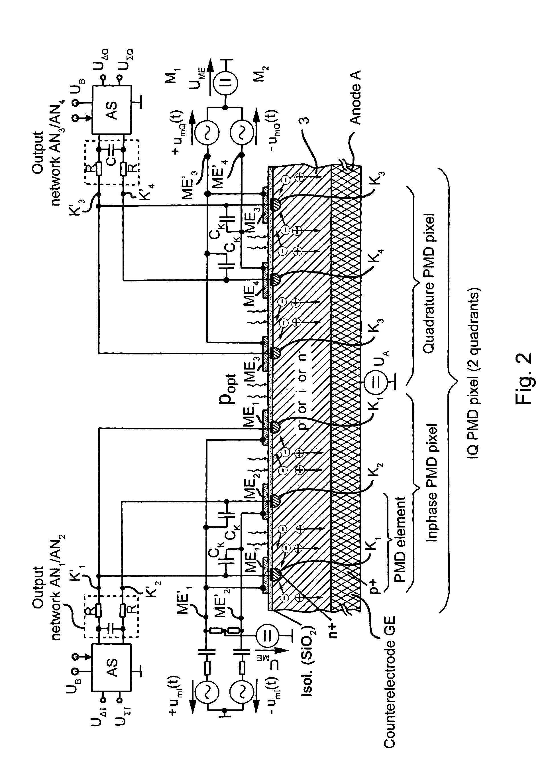
[0022]The aforesaid object of the invention is achieved by the features of process claim 1, by specifying this process specifically for different signal waves, and by the subsequent device claims for carrying out the process. This invention is based on the knowledge that a common receiving process independent of the type of signal waves consists of a demodulating push-pull oscillation process and can be carried out advantageously on an industrial scale, and that for optical signal waves or photocharges generated by same in a modification of the known process, such an oscillation process is not dependent on the use of photogates in the CMOS and CCD photogate PMDs, and that for different optical problem definitions, novel, very advantageous alternative PMD processes and corresponding PMD realizations can be named, and that this demodulating push-pull oscillation process can be used on very different types of signal waves such as microwaves and ultrasonic waves and X-rays, and that cor...


PUM


Abstract

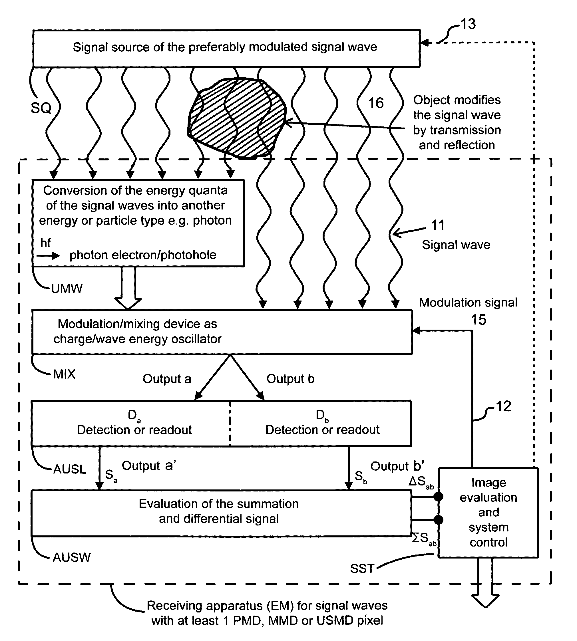
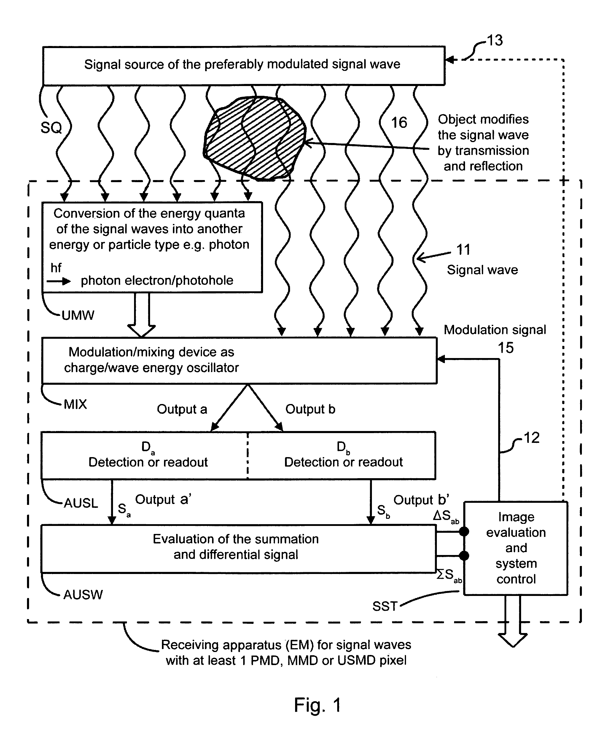
The invention relates to a method for detecting and processing the amplitude and phase of signal waves. A Modulated signal source generates the signal waves which are modified by transmission medium or by reflection and scattering by at least one object. The modified signal waves are received and demodulated using a modulation signal. The amplitude of the modulated signal waves and their phase relationship to the modulation signal are measured and evaluated. The demodulated signal wave is converted into an electrical charge or charge displacement in the receiving medium and is distributed in accordance with a modulation signal to at least two readout outputs and fed to an evaluation unit. The evaluation unit produces the sum and difference of the output signals thus applying the value of the intensity and the phase position of the signal wave that has been scattered, reflected or delayed by the object.

Description

FIELD OF THE INVENTION[0001]The present invention relates to a method for detecting and processing the amplitude and phase of signal waves, in particular of electromagnetic waves in the total range of microwaves from heat radiation to gamma radiation (X-rays), furthermore of acoustic waves or ultrasonic waves and also of other current, voltage or charge-generating radiation signals, hereafter shortened to “signal waves” and, depending on the respective application, also acoustic, optic, electromagnetic signal waves, X-ray waves or microwaves, according to the precharacterizing clause of claim 1, and also devices for carrying out the process.BACKGROUND OF THE INVENTION[0002]An important technical task in industrial production and automation, in metrology, in road traffic, in safety engineering, environmental technology and many additional fields, consists of obtaining, via the propagation of signal waves, i.e. contact-less by means of wave propagation either passively (externally-gen...

Claims


Application Information

Patent Timeline
IPC IPC(8): G01J9/00G02F2/00H01L27/14G01S7/4914G01S17/894H01L31/10H01L31/107H01L31/108H03D1/00H03D9/06H04L27/00
CPCG01S7/4914H03D9/0608G02F2/002G01S17/89G01S17/894G01R19/00
Inventor SCHWARTE, RUDOLF
Owner SCHWARTE RUDOLF
Learn More