One-way switch
a one-way switch and switch technology, applied in the field of one-way switches, can solve the problems of limiting its application, difficult to reduce, intrinsic defects,
- Summary
- Abstract
- Description
- Claims
- Application Information
AI Technical Summary
Benefits of technology
Problems solved by technology
Method used
Image
Examples
first embodiment
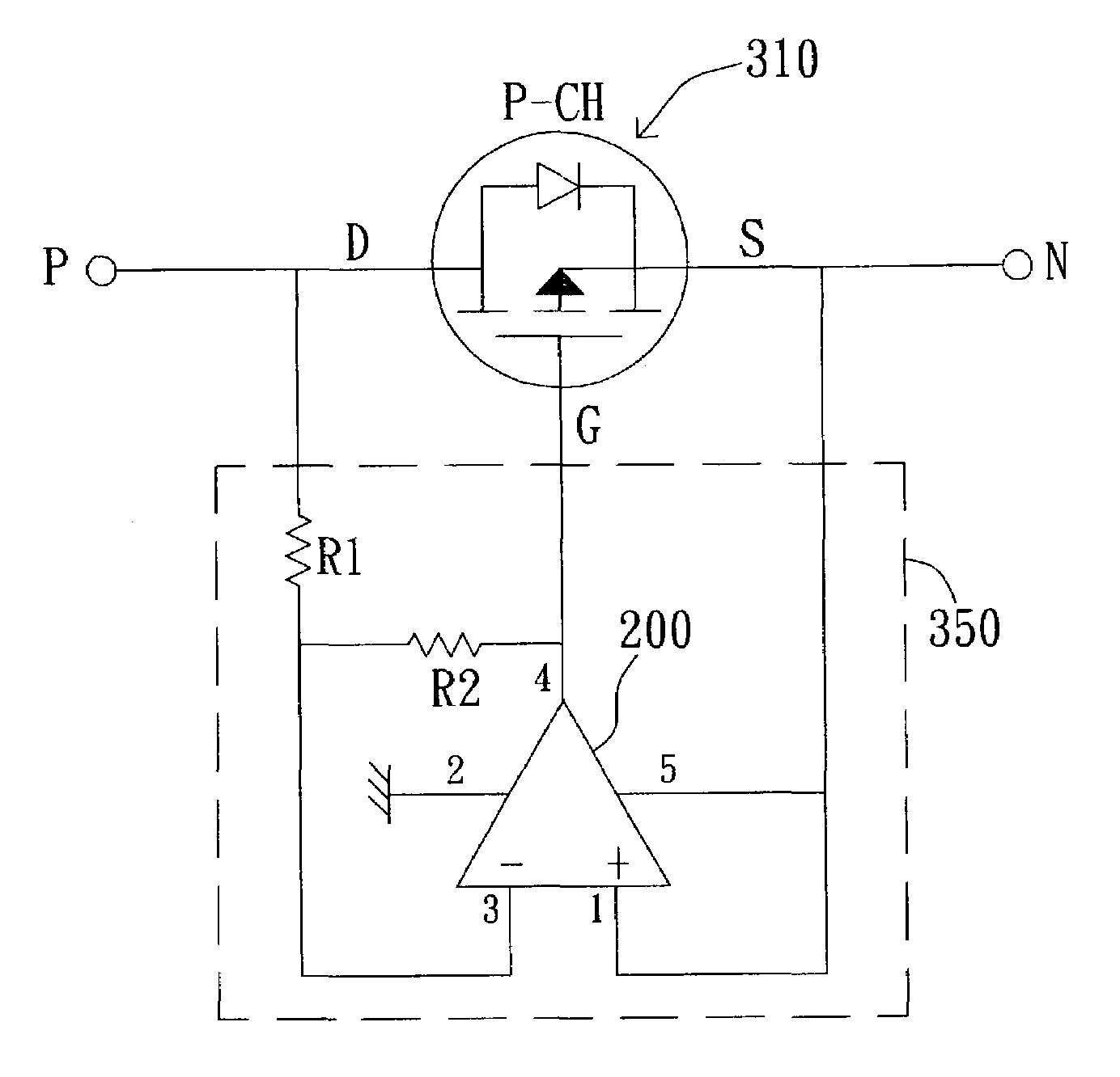
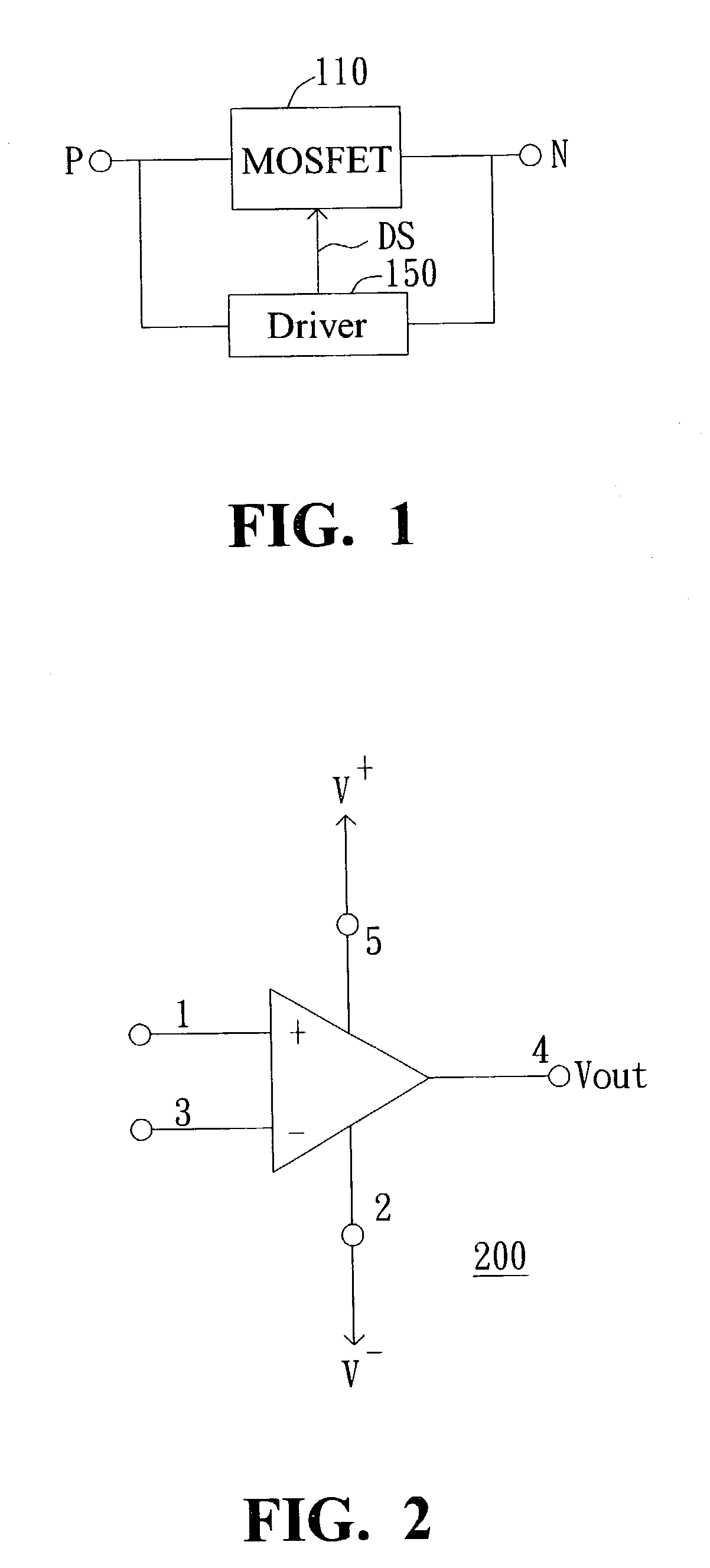
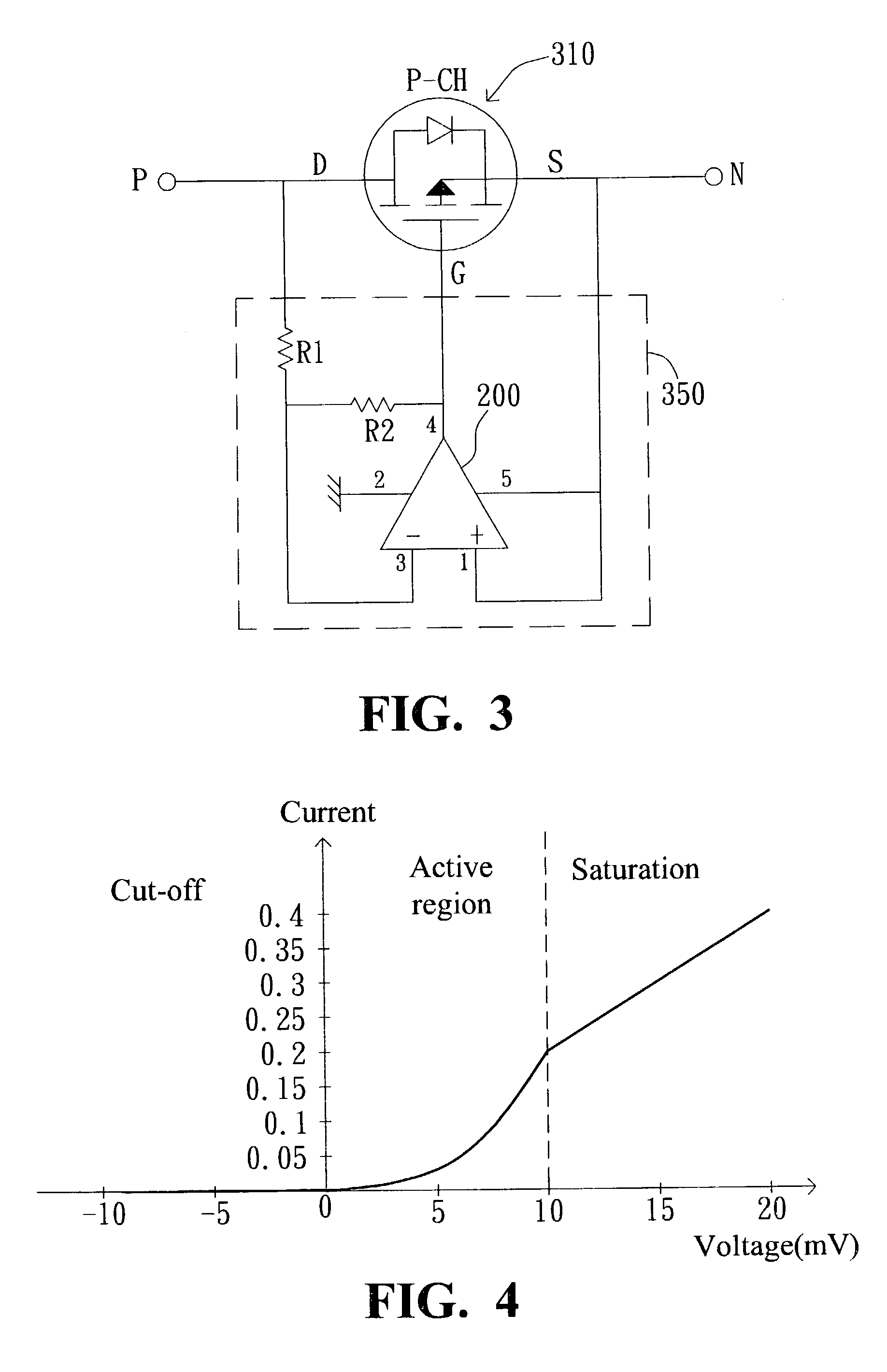
[0016]When a metal oxide semiconductor field effect transistor (MOSFET) is turned on, the forward voltage between drain and source is pretty low. If the metal oxide semiconductor field effect transistor can be modified to work in one single direction, the metal oxide semiconductor field effect transistor can have all functions of the diode and work even better. It is known with the ones skilled in the art that the typical diode has P-terminal and N-terminal. Ideally, when the P-terminal voltage is higher than the N-terminal voltage, the diode is turned on, which is equivalent to short circuit. When the P-terminal voltage is lower than the N-terminal potential, the diode is turned off, which is equivalent to open circuit. Therefore, the diode has the characteristic of working in one direction. The one-way switch provided by the present invention also has a P-terminal and an N-terminal and it also has the characteristic of working in one direction. The detailed description of the one-...
second embodiment
[0025]Referring to FIG. 6, it shows a circuit diagram of another one-way switch according to the second embodiment of the present invention. The one-way switch comprises a MOSFET 610 and a driver 650 coupled with each other. The MOSFET 610 is an N channel transistor, i.e. NMOS. The source S and the drain D function as P-terminal and N-terminal. The driver 650 is an inverting amplifier composed of an operation amplifier 200, a resistor R1 and a resistor R2. The non-inverting input terminal 1 is coupled to the source S, the output terminal 4 is coupled to the gate G, the inverting input terminal 3 is coupled to one terminal of the resistor R1, and the other terminal of the resistor R1 is coupled to the drain D. One terminal of the resistor R2 is coupled the inverting input terminal 3, and the other terminal of the resistor R2 is coupled to the output terminal 4. The high power terminal 5 is coupled to the power V+which has higher voltage than the source S. The low power terminal 2 is ...
PUM
 Abstract
Description
Claims
Application Information
 - Generate Ideas
- Intellectual Property
- Life Sciences
- Materials
- Tech Scout
- Unparalleled Data Quality
- Higher Quality Content
- 60% Fewer Hallucinations
Browse by: Latest US Patents, China's latest patents, Technical Efficacy Thesaurus, Application Domain, Technology Topic, Popular Technical Reports.
© 2025 PatSnap. All rights reserved.Legal|Privacy policy|Modern Slavery Act Transparency Statement|Sitemap|About US| Contact US: help@patsnap.com


