
Circuit and method to match common mode flex impedance and to achieve symmetrical switching voltage outputs of write driver

a technology of write driver and common mode flex impedance, which is applied in logic circuit coupling/interface arrangement, pulse technique, instruments, etc., can solve the problems of limiting the data rate of the disk drive system and severe signal reflection, and achieve low interference in the disk drive system. jitter and low interferen

Inactive Publication Date: 2006-02-28
TEXAS INSTR INC
View PDF19 Cites 18 Cited by
  • Summary
  • Abstract
  • Description
  • Claims
  • Application Information

AI Technical Summary

Benefits of technology

[0006]The present invention is directed to a system and method for matching both the differential and common mode impedance of a disk drive system write driver to a flex / interconnect impedance to achieve minimal signal reflections and permit very high data rates associated with write operations.
[0008]In another aspect of the invention, a system and method for matching both the differential and common mode impedance of a disk drive system write driver to a flex / interconnect impedance is implemented to achieve low jitter and low interference in the disk drive system.

Problems solved by technology

When writing at high data rates (e.g. 1–2 Gb / s), the mismatch of the differential and common mode impedance between the write driver's output and the flex / interconnect input impedance causes severe signal reflections.
These differential and common mode reflections degrade the integrity of the signal written onto the thin film transducer, which in turn limits the data rate of the disk drive system.

Method used


Image

  • Circuit and method to match common mode flex impedance and to achieve symmetrical switching voltage outputs of write driver
  • Circuit and method to match common mode flex impedance and to achieve symmetrical switching voltage outputs of write driver
  • Circuit and method to match common mode flex impedance and to achieve symmetrical switching voltage outputs of write driver

Examples


Embodiment Construction

[0017]As stated herein before, when a write driver in a disk drive system is used to write data into a thin film transducer, a flex / interconnect is commonly used to connect the output of the write driver to the thin film transducer. When writing at high data rates (e.g. 1–2 Gb / s), the mismatch of the differential and common mode impedance between the write driver's output and the flex / interconnect input impedance causes severe signal reflections. These differential and common mode reflections degrade the integrity of the signal written onto the thin film transducer, which in turn limits the data rate of the disk drive system.

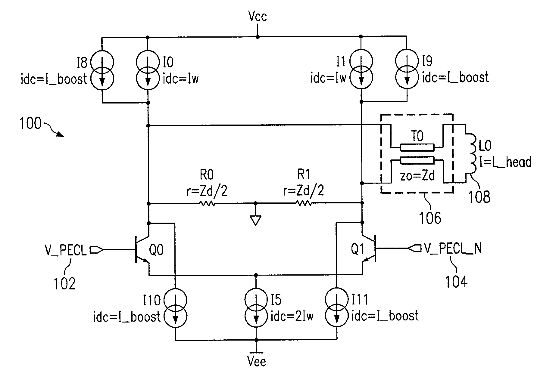
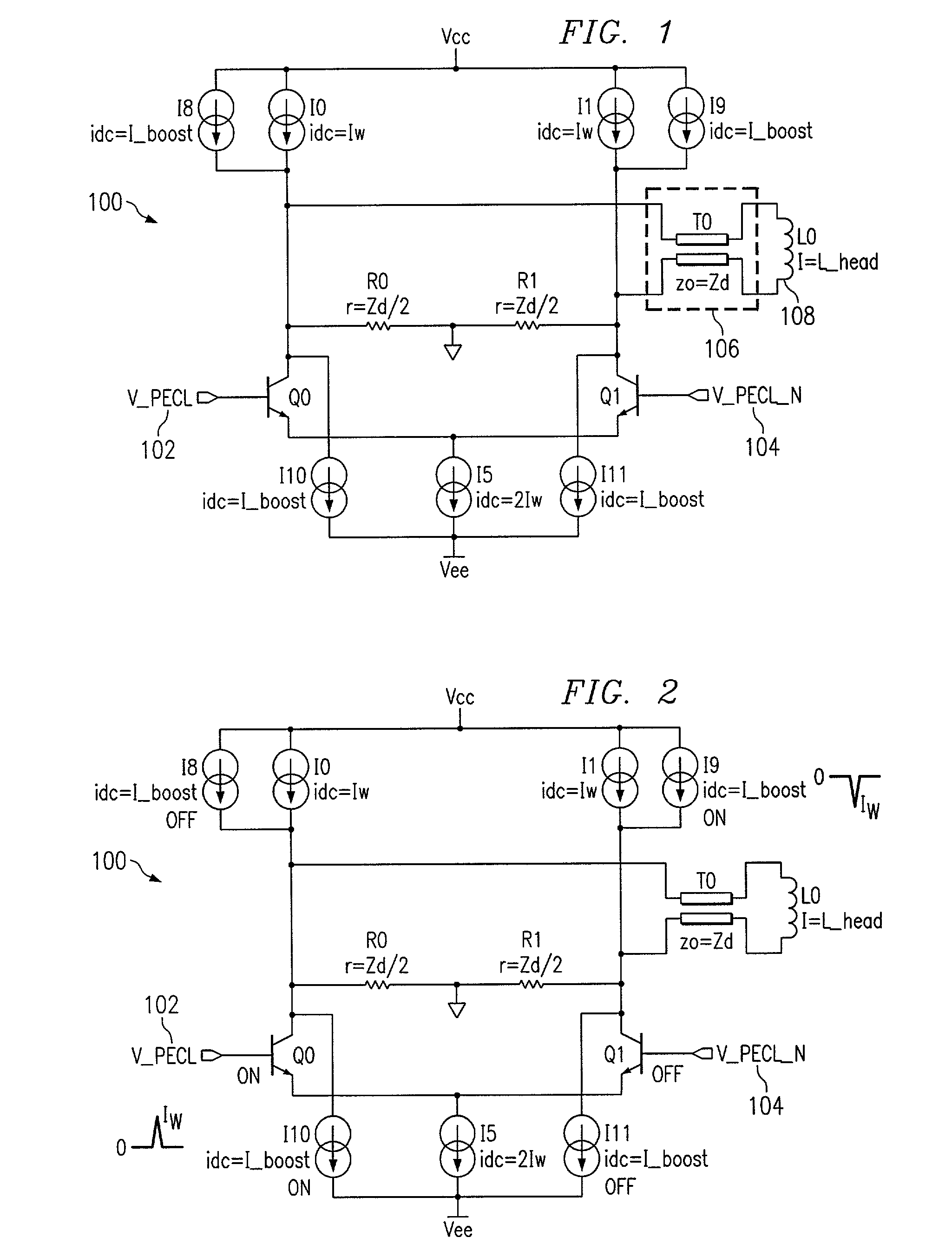
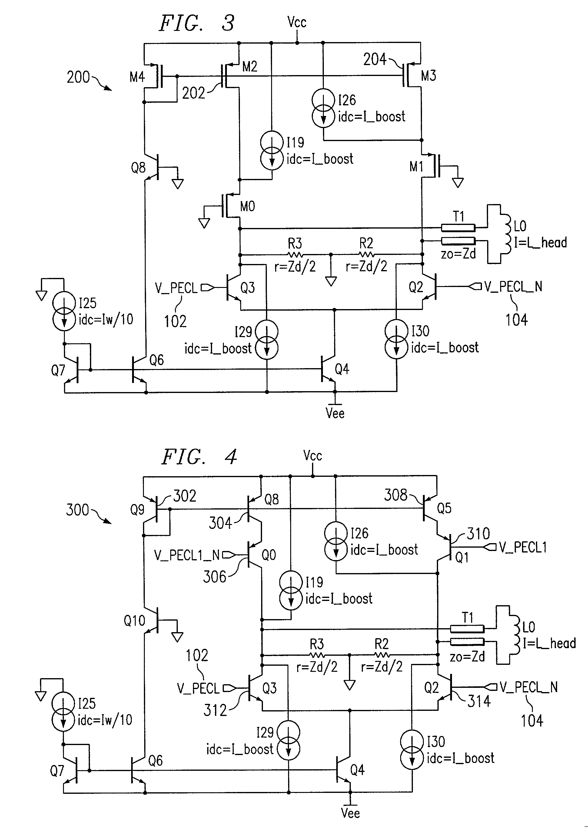
[0018]Looking now at FIG. 1, a schematic diagram illustrates a current mode impedance matched write driver (current switch) 100 for an inductive head (thin film transducer) 108 associated with a disk drive system using PECL logic according to one embodiment of the present invention. The differential output impedance of the current-mode write driver 100 is matche...


PUM

PropertyMeasurementUnit
supply voltagesaaaaaaaaaa
voltageaaaaaaaaaa

Abstract

A write driver 100, 200, 300 is implemented to provide near-ground common mode output voltages to produce a more symmetrical head voltage swing (i.e. ±0.4V from ground to ±5V supply voltages). These features help to reduce the effects of common mode impedance associated with the interconnection to the disk drive head to improve overall performance. Lower jitter at high data rates can be achieved when compared to prior art techniques for implementing current mode write drivers. Further, the matched impedance between the write driver 100 and the interconnection 106 eliminates unwanted reflections. ECL level voltage swings (200–500 mV) have replaced more conventional CMOS level voltage swings (5V) to further reduce overall power dissipation associated with the write driver. The small ECL level switching further maintains constant power dissipation with changes in operating frequency and results in less NTLS effects due to quieter supplies.

Description

BACKGROUND OF THE INVENTION[0001]1. Field of the Invention[0002]This invention relates generally to write drivers, and more particularly, to a technique for matching both the differential and common mode impedance of a write driver to a line (i.e. flex / interconnect) impedance.[0003]2. Description of the Prior Art[0004]When a write driver in a disk drive system is used to write data into a thin film transducer, a flex / interconnect is commonly used to connect the output of the write driver to the thin film transducer. When writing at high data rates (e.g. 1–2 Gb / s), the mismatch of the differential and common mode impedance between the write driver's output and the flex / interconnect input impedance causes severe signal reflections. These differential and common mode reflections degrade the integrity of the signal written onto the thin film transducer, which in turn limits the data rate of the disk drive system.[0005]In view of the foregoing, it would be desirable and advantageous in t...

Claims


Application Information

Patent Timeline
Patent Type & Authority Patents(United States)
IPC IPC(8): G11B5/09G11B5/00G11B5/012G11B5/02H03K17/66H03K19/0175
CPCG11B5/012G11B5/02H03K17/663G11B5/022G11B2005/001G11B2005/0013
Inventor NGO, TUAN V.
Owner TEXAS INSTR INC
Learn More