Organic electroluminescence element and manufacturing method thereof
a technology of electroluminescence elements and organic elements, which is applied in the direction of discharge tubes/lamp details, organic semiconductor devices, discharge tubes/lamp details, etc., can solve the problems of difficult to produce organic el elements with a large area, difficult to effectively obtain blue light from electrodes, and limited electrode material, etc., to prevent short circuits
- Summary
- Abstract
- Description
- Claims
- Application Information
AI Technical Summary
Benefits of technology
Problems solved by technology
Method used
Image
Examples
first embodiment
[First Embodiment]
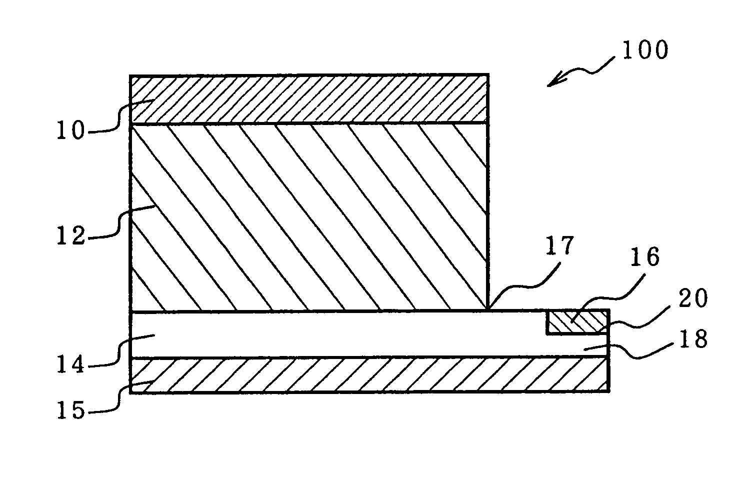
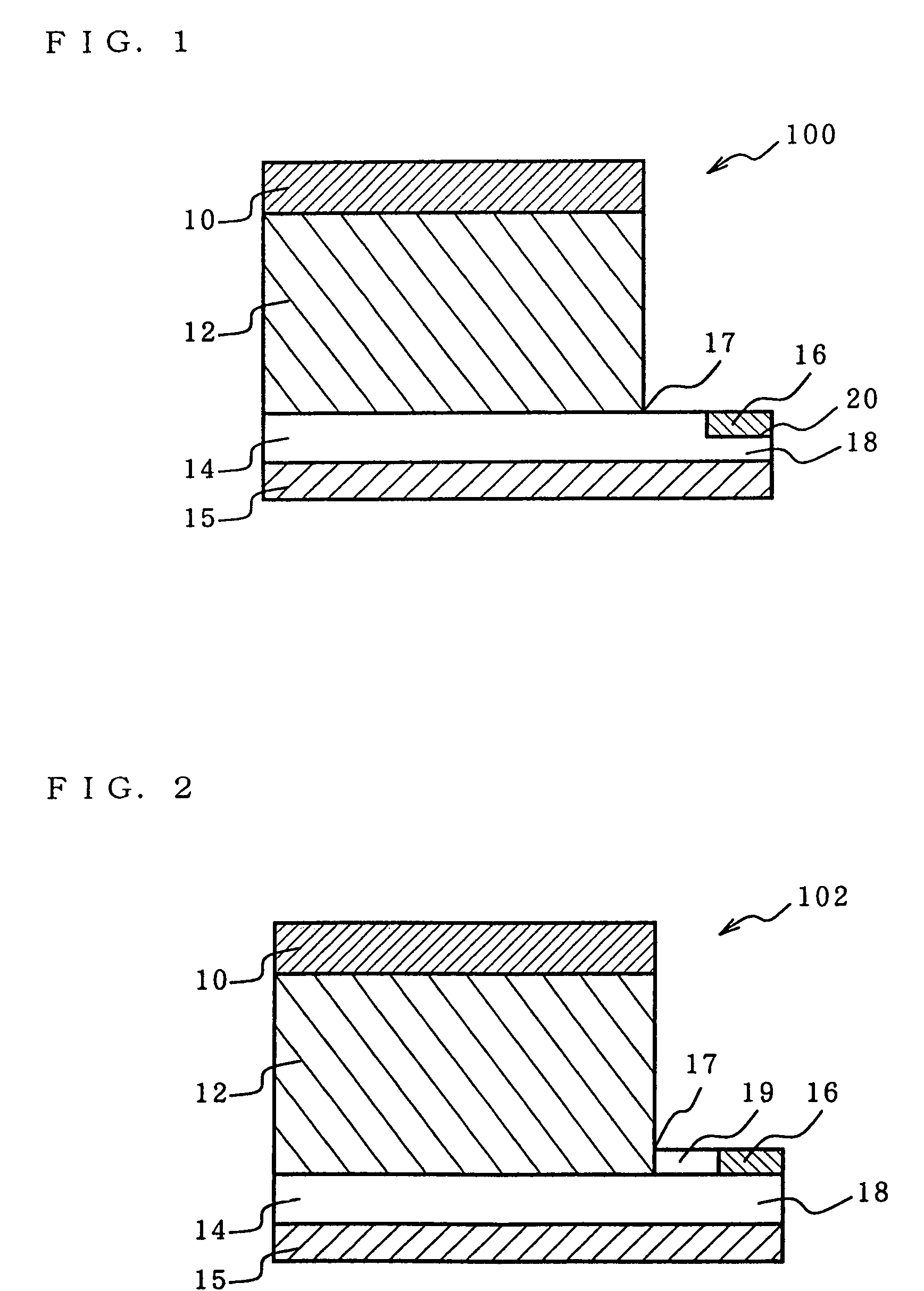
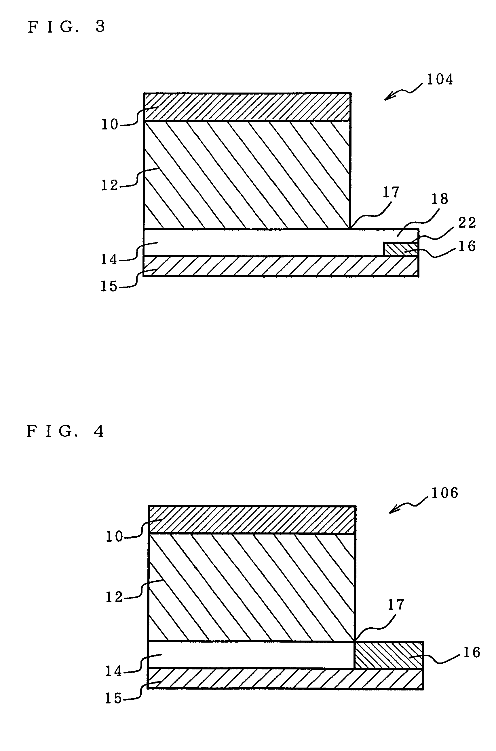
[0081]Referring now to FIG. 1, the first embodiment according to the present invention will be described. FIG. 1 is a cross-sectional view of an organic EL element in the first embodiment, wherein on the support substrate 15, a semiconductor layer 14 comprising non-monocrystal material, an organic light-emitting medium 12, and a cathode (first cathode) 10 are formed successively. To the extension 18 extended in the horizontal section from the edge section 17 of the semiconductor layer 14, the anode (second electrode) 16 is electrically connected.
[0082]Consequently, as the light may be taken out from the semiconductor layer 14 to the outside by configuring in this way, the light energy (or light intensity) can be increased. In addition, since the anode (second electrode) 16 and the cathode (first electrode) are not practically opposite to each other, a wide variety of electrode materials may be used and the electrical connection to the outside is facilitated. In add...
second embodiment
[Second Embodiment]
[0178]Referring now to FIG. 12(a) to FIG. 12(d), the manufacturing method of an organic EL element which is the second embodiment according to the present invention will be described in detail.
[0179]FIG. 12(a)–(d) is illustrations that schematically show the organic EL element in each process (step) of the manufacturing method related to the second embodiment. In the following discussion, the manufacturing method of the organic EL element is focused, and with respect to the component materials, and the like, the contents described for the first embodiment may apply.
(i) Formation of Anode (Second Electrode)
[0180]FIG. 12(a) shows the condition in which the anode (second electrode) 16 is installed on the support substrate 15.
[0181]The method for forming this anode 16 is not particularly limited, but the anode may be able to be formed in the specified location by combining sputtering (deposition method) and photolithography. Specifically, on the support substrate 15, ...
example 1
(1) Fabrication of Organic EL Element
(i) Formation of the Cathode (Second Electrode)
[0192]A transparent glass substrate having a dimension of 1.1 mm(thickness)×200 mm(length)×200 mm (width) was ultrasonically cleaned and after drying in the N2 (nitrogen gas) environment, the glass substrate was cleaned by the use of UV (ultraviolet ray) and ozone further for 10 minutes. Then, on the cleaned glass substrate, a thin film (100 nm thick) comprising Al / Si alloy (Si concentration: 1 at. %) was formed by the use of the sputtering apparatus (available from ULVAC JAPAN, Ltd.). This Al / Si alloy thin film was patterned in lattices (line width: 20 μm; lattice pitch: 320 μm) by the use of photolithography as shown in FIG. 11(a). The construction of the configuration in which the cathode (second electrode) was electrically connected at the edge section of the semiconductor layer was intended.
(ii) Formation of the Semiconductor Layer
[0193]The glass substrate on which the cathode was formed was cle...
PUM
 Abstract
Description
Claims
Application Information
 - R&D
- Intellectual Property
- Life Sciences
- Materials
- Tech Scout
- Unparalleled Data Quality
- Higher Quality Content
- 60% Fewer Hallucinations
Browse by: Latest US Patents, China's latest patents, Technical Efficacy Thesaurus, Application Domain, Technology Topic, Popular Technical Reports.
© 2025 PatSnap. All rights reserved.Legal|Privacy policy|Modern Slavery Act Transparency Statement|Sitemap|About US| Contact US: help@patsnap.com


