
Practical methodology for early buffer and wire resource allocation

a technology of wire resource allocation and early buffer placement, which is applied in the field of early buffer placement in an integrated circuit, can solve the problems of affecting affecting the design of application specific integrated circuits (asics), and affecting the timing of the timing closure process,

Inactive Publication Date: 2006-02-07
IBM CORP
View PDF11 Cites 60 Cited by
  • Summary
  • Abstract
  • Description
  • Claims
  • Application Information

AI Technical Summary

Benefits of technology

The present invention is a method, system, and computer program product for placing buffer and wire in an integrated circuit design. It uses a tile graph representation of the surface of the circuit design and a cost minimization algorithm to route nets and assign buffer locations to them. This helps to efficiently allocate resources and minimize the overall cost of the circuit design.

Problems solved by technology

Achieving timing closure becomes more difficult when buffer insertion is deferred to the back end of the design process, and the buffers must be squeezed into whatever left over space remains.
The problem is particularly acute for custom designs, where large IP core macros and custom data flow structures are present, blocking out significant areas from buffering possibilities.
Application Specific Integrated Circuit (ASIC) designs can also run into similar headaches if they are dense, or have locally dense hot spots.
In addition, design routability has also become a critical problem; one must make sure that an achievable routing solution exists during the physical floorplanning stage.
There are two fundamental problems with this buffer block planning approach:I.
As more and more wires are needed, it is the routing resources that become contentious.
Therefore, the design may not be routable due to heavy congestion between functional blocks 101–110.II.
Buffers must be placed in poor locations since better locations are blocked.
For example, signal integrity could degrade beyond the point of recovery or wire delay may simply be too high.
Ultimately this methodology will not be sustainable as design complexity continues to increase.
Clumping buffers together, e.g., in buffer blocks, or between abutting macros invites routing headaches.

Method used


Image

  • Practical methodology for early buffer and wire resource allocation
  • Practical methodology for early buffer and wire resource allocation
  • Practical methodology for early buffer and wire resource allocation

Examples


Embodiment Construction

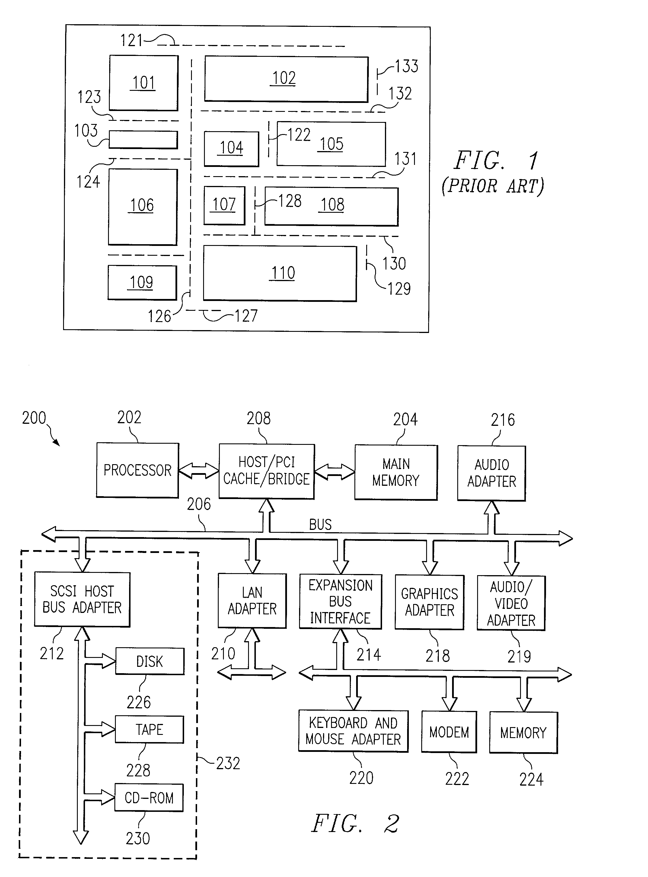
[0028]With reference now to FIG. 2, a block diagram illustrating a data processing system is depicted in which the present invention may be implemented. Data processing system 200 is an example of a data processing system that may be used to implement a computer program product for designing buffer block placement in an integrated circuit chip in accordance with the present invention. Data processing system 200 employs a peripheral component interconnect (PCI) local bus architecture. Although the depicted example employs a PCI bus, other bus architectures such as Accelerated Graphics Port (AGP) and Industry Standard Architecture (ISA) may be used. Processor 202 and main memory 204 are connected to PCI local bus 206 through PCI bridge 208. PCI bridge 208 also may include an integrated memory controller and cache memory for processor 202. Additional connections to PCI local bus 206 may be made through direct component interconnection or through add-in boards.

[0029]In the depicted exam...


PUM


Abstract

A method, system, and computer program product for allocating buffer and wire placement in an integrated circuit design is provided. In one embodiment, the surface of a integrated circuit design is represented as a tile graph. Allocation of buffer locations for selected tiles in the tile graph is then received and nets are routed between associated sources and sinks. Buffer locations within selected tiles are then selectively assigned based upon buffer needs of the nets, wherein the nets are routed through selected tiles and assigned buffer locations using a cost minimization algorithm.

Description

BACKGROUND OF THE INVENTION[0001]1. Technical Field[0002]The present invention relates to integrated circuit (IC) chip design and, more particularly, to methods of designing buffer placement in an IC chip.[0003]2. Description of Related Art[0004]Buffer insertion has become a critical step in deep submicron design as interconnect now plays a dominating role in determining system performance. The insertion of buffers and inverters on signal nets can provide several advantages, including reducing interconnect delay, restraining noise, improving the slew rate, and fixing electrical violations. Current designs easily require thousands of nets to be buffered, and it is speculated that close to 800,000 buffers will be required for chip designs in 70 nanometer technology for a microprocessor chip with 500 million transistors.[0005]Achieving timing closure becomes more difficult when buffer insertion is deferred to the back end of the design process, and the buffers must be squeezed into wha...

Claims


Application Information

Patent Timeline
Patent Type & Authority Patents(United States)
IPC IPC(8): G06F17/50G06F9/45
CPCG06F17/5072G06F30/392
Inventor ALPERT, CHARLES JAYHU, JIANGVILLARRUBIA, PAUL GERARD
Owner IBM CORP
Learn More