Coated spherical silicon nanoparticle thin film UV detector with UV response and method of making

a thin film, spherical silicon technology, applied in the direction of nanostructure manufacturing, optical radiation measurement, photometry, etc., can solve the problems of large number, large number, and general usefulness of elastic silicon for uv detection

Inactive Publication Date: 2006-01-31
THE BOARD OF TRUSTEES OF THE UNIV OF ILLINOIS
View PDF28 Cites 21 Cited by
  • Summary
  • Abstract
  • Description
  • Claims
  • Application Information

AI Technical Summary

Benefits of technology

[0008]A UV detector has a UV detection thin film of coated spherical silicon nanoparticles formed upon a substrate. The spherical silicon nanoparticles in a UV detection film of the invention have sizes selected from the group of 1 nm, 1.67nm, 2.15 nm 2.9 nm and 3.7 nm. The coating can determine wavelength sensitivity. The detector includes structures to bias the thin film. A thin conductor that is at least semi-transparent to UV radiation is formed over the UV detection thin film. In preferred embodiments, the UV detector is formed as a silicon based integration, upon a device quality silicon wafer.

Problems solved by technology

These are unsuitable in many cases due to slow response time, size constraints, and due to the demanding environments in which UV detectors, in some cases, may find utility.
Elemental silicon is not generally useful for UV detection because it has a bandgap of 1.1 eV, corresponding to an infrared wavelength of 1.1 μm.
Si is accordingly not fit for UV detection, necessitating the use of other materials, such as nitride-based heterostructures grown on incompatible substrates, namely Si and Ge.
Fabrication on Si leads to a large number of defects, which can impact device sensitivity and general performance.

Method used


Image

  • Coated spherical silicon nanoparticle thin film UV detector with UV response and method of making
  • Coated spherical silicon nanoparticle thin film UV detector with UV response and method of making
  • Coated spherical silicon nanoparticle thin film UV detector with UV response and method of making

Examples


Embodiment Construction

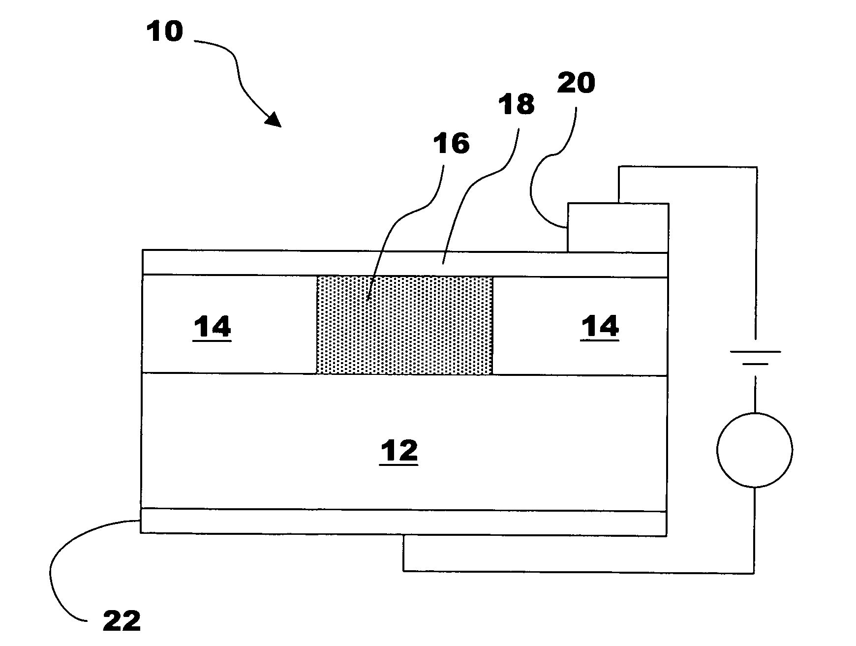
[0013]The invention will be illustrated with respect to preferred embodiment devices. In general, UV detection films of the invention may find use in various semiconductor device structures. These include various detector structures, e.g. photodetectors, and also the incorporation of detector structures of the invention into device integrations.

[0014]The invention provides a stable and high performance silicon based UV light detector. A detector of the invention exhibits photostablity. Detectors of the invention may be produced with an arbitrarily large active area, e.g., 1 cm2, as the physical nature of the stable UV detection films of the invention does not limit the active area size. Methods of forming detectors of the invention do not require lithographic or epitaxial techniques to form the coated spherical silicon nanoparticle UV sensitive thin film. This is a manufacturing advantage and makes devices of the invention amenable to large-volume production and wide scale integrati...


PUM

PropertyMeasurementUnit
sizesaaaaaaaaaa
sizesaaaaaaaaaa
sizesaaaaaaaaaa

Abstract

A UV detector has a UV detection thin film of coated spherical silicon nanoparticles formed upon a substrate. The detector includes structures to bias the thin film. In preferred embodiments, a thin conductor that is at least semi-transparent to UV radiation is formed over the thin film. In preferred embodiments, the UV detector is formed as a silicon based integration, upon a device quality silicon wafer.

Description

RELATED APPLICATION AND PRIORITY CLAIMED[0001]This application is a continuation-in-part of application Ser. No. 09 / 990,250, filed Nov. 21, 2001, now U.S. Pat. No. 6,743,406 entitled “Family of Discretely Sized Silicon Nanoparticles and Method for Producing the Same”. Priority is claimed under 35 U.S.C. § 120.STATEMENT OF GOVERNMENT INTEREST[0002]This invention was made with Government assistance under NSF Grant No. BES-0118053. The Government has certain rights in this invention.FIELD OF THE INVENTION[0003]A field of the invention is UV radiation detection.BACKGROUND OF THE INVENTION[0004]Detection of ultraviolet (UV) radiation is an important feature for many applications. Sensitive UV light detection may find applications as diverse as military, security, commercial, and consumer applications.[0005]UV detection may make use of the photoelectric effect of metal and the gas multiplication effect. Many commercial UV detectors take the form of gas tubes. These are unsuitable in many ...

Claims


Application Information

Patent Timeline
Patent Type & Authority Patents(United States)
IPC IPC(8): G01J1/42H01L21/00H01L27/14H01L31/00B82B3/00C01B33/02C01B33/021C25F3/12G01J1/04G02B6/02G02B6/10H01L29/06H01L29/66H01L31/0352H01L31/115H01S3/16H01S5/04H01S5/10H01S5/30
CPCB82Y30/00C01B33/02G01J1/04G01J1/0407G01J1/429H01L31/035281H01S5/30H01L31/115Y02E10/50H01S3/163H01S5/041H01S5/10H01S5/3031
Inventor NAYFEH, MUNIR H.NAYFEH, OSAMA M.
Owner THE BOARD OF TRUSTEES OF THE UNIV OF ILLINOIS
Why Eureka
Try Eureka