Semiconductor device having DAC channels for video signals
a technology of video signal and semiconductor device, which is applied in the field of semiconductor device having dac channel for video signal, can solve the problems of image associated degradation, difficult separation of luminance signal y from chrominance signal c, and degradation of picture quality, so as to reduce source voltage fluctuations and prevent degradation of picture quality
- Summary
- Abstract
- Description
- Claims
- Application Information
AI Technical Summary
Benefits of technology
Problems solved by technology
Method used
Image
Examples
first embodiment
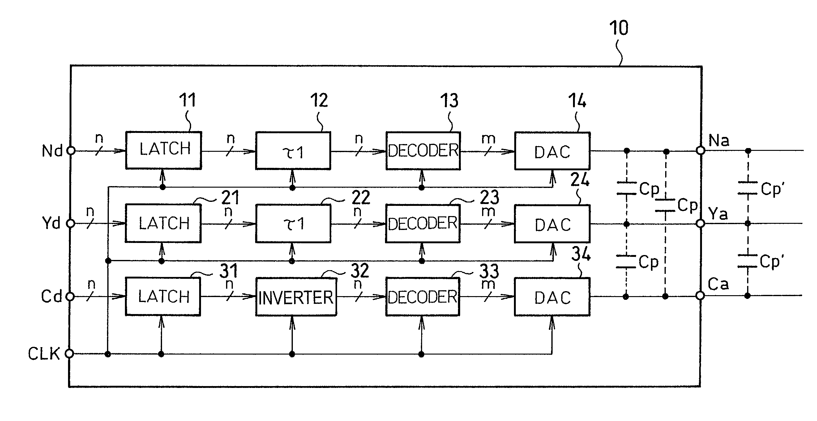
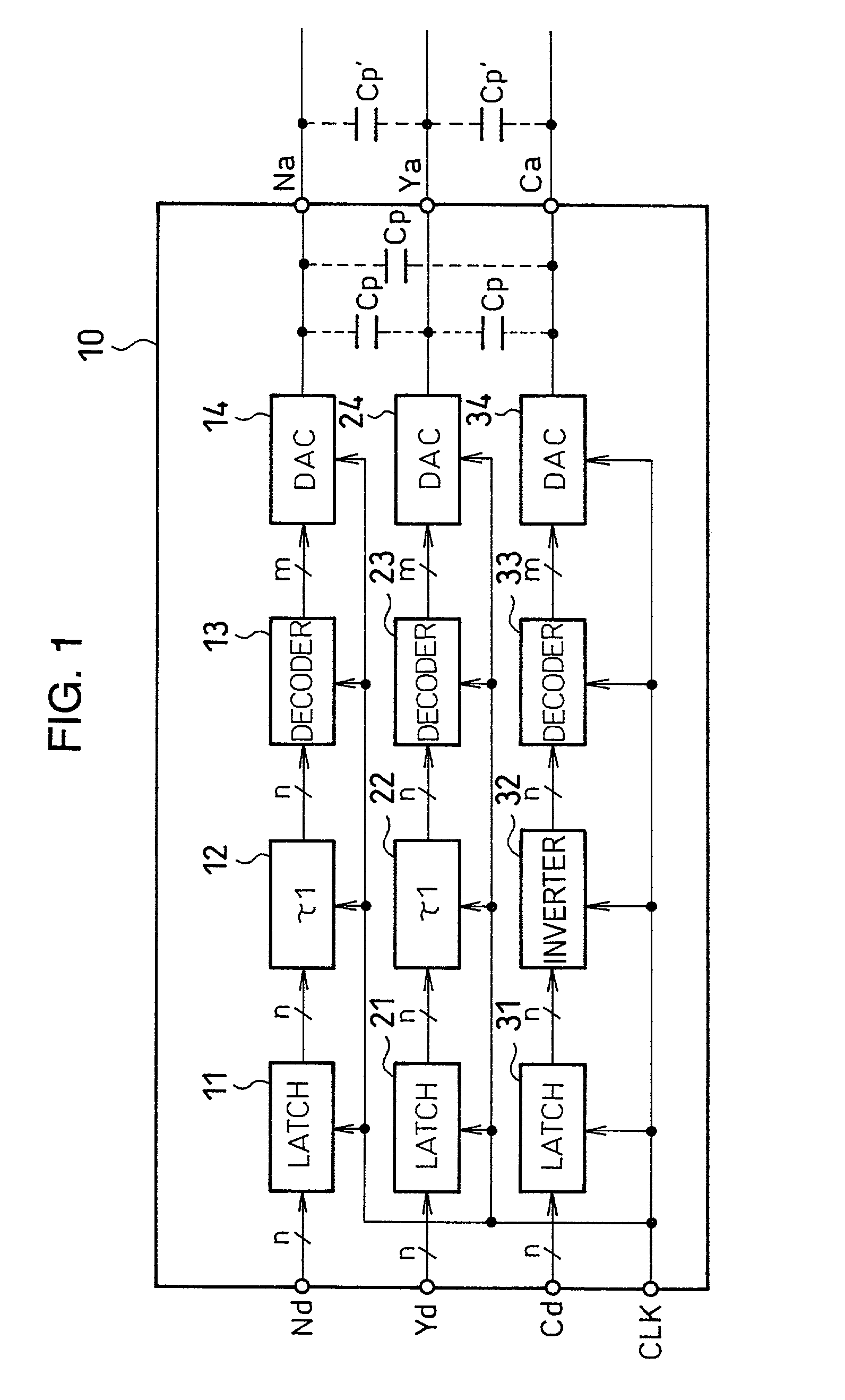
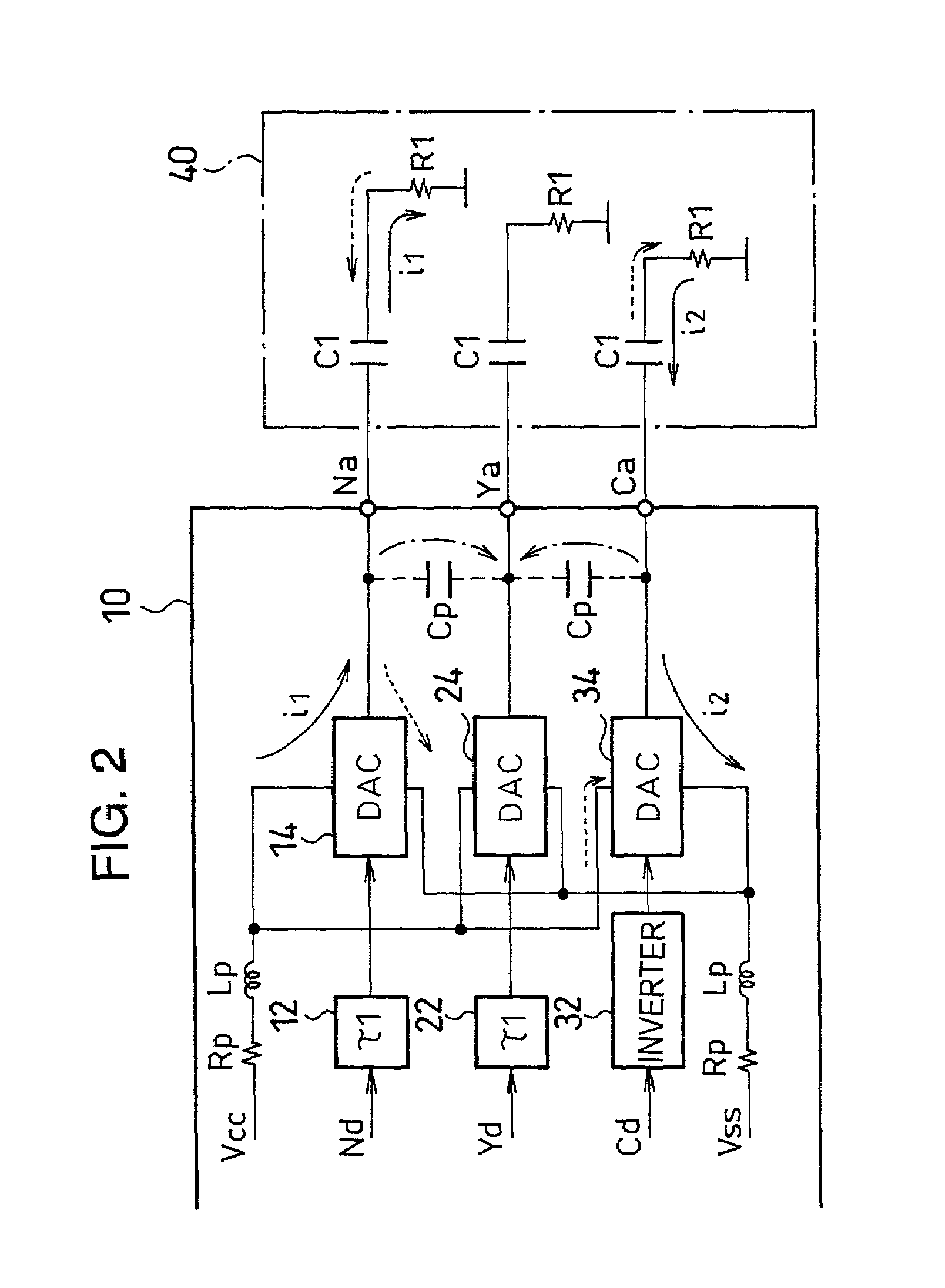
[0034]Referring now to FIG. 1, there is shown a section of a semiconductor device 10 relevant to DACs for video signals according to the invention. Functions of the device are illustrated in the circuit diagram shown in FIG. 2. Waveforms appearing in the circuit are shown in FIGS. 3A–3C.
[0035]As shown in FIG. 1, an n-bit digital composite signal Nd in NTSC system or PAL system includes all the necessary signals for a color image, such as a luminance signal Y, a chrominance signal C for orthogonal phase modulations of a first color difference signal B-Y and a second color difference signal R-Y by a subcarrier wave (having a frequency of 3.58 MHz in NTSC system and 4.43 MHz in PAL system), and horizontal and vertical synchronization signals. It is assumed hereinafter that the number of bits n can be 10 for example, unless otherwise stated. In the example shown herein a digital luminance signal Yd includes horizontal and vertical synchronization signals. Digital chrominance signal Cd f...
second embodiment
[0066]Referring to FIG. 4, there is shown a relevant portion of a semiconductor device 50 having DACs according to the invention. FIG. 5 shows a circuit diagram illustrating functions of the device 50. FIGS. 6A–6C illustrate waveforms of analog signals generated by the device 50.
[0067]A first digital luminance signal Yd1, a digital composite signal Nd, a digital chrominance signal Cd, and a system clock CLK shown in FIG. 4 are the same as the corresponding signals shown in FIG. 1.
[0068]A second digital luminance signal Yd2 is the same as the first digital luminance signal Yd1. Together with the second digital luminance signal Yd2, a first digital color difference signal Ud (B-Y) and a second digital color difference signal Vd (R-Y) form a group of three color signals. In this group of color signals, the luminance signal is separately formed from the respective color difference signals that Y / C separation nor the separation of the chrominance signal is needed. Hence, a high resolutio...
PUM
 Abstract
Description
Claims
Application Information
 - R&D
- Intellectual Property
- Life Sciences
- Materials
- Tech Scout
- Unparalleled Data Quality
- Higher Quality Content
- 60% Fewer Hallucinations
Browse by: Latest US Patents, China's latest patents, Technical Efficacy Thesaurus, Application Domain, Technology Topic, Popular Technical Reports.
© 2025 PatSnap. All rights reserved.Legal|Privacy policy|Modern Slavery Act Transparency Statement|Sitemap|About US| Contact US: help@patsnap.com


