
Semiconductor device in which a semiconductor chip mounted on a printed circuit is sealed with a molded resin

a semiconductor chip and printed circuit technology, applied in the direction of printed circuit manufacturing, printed circuit non-printed electric components association, non-metallic protective coating application, etc., can solve the problem of optic semiconductor chip fluctuation of light incident to optic semiconductor chip, reduced reliability of semiconductor device including optic semiconductor chip, and difficulty in directing light to target position on optic semiconductor chip, etc. problem, to prevent the occurrence of cracks and/or peeling o

Inactive Publication Date: 2005-12-06
RENESAS ELECTRONICS CORP
View PDF30 Cites 0 Cited by
  • Summary
  • Abstract
  • Description
  • Claims
  • Application Information

AI Technical Summary

Benefits of technology

[0021]In view of the above-mentioned problem in the conventional semiconductor device, it is an object of the present invention to provide a sealed type semiconductor device including a semiconductor chip mounted on a printed wiring board and sealed with a molded resin, which semiconductor device is capable of preventing occurrence of crack and / or peeling off therein, even if the semiconductor device is subject to a heating step such as a re-flow step.

Problems solved by technology

A semiconductor device including such an optic semiconductor chip could have reduced reliability relative to a semiconductor device including a semiconductor chip sealed with a filler-containing resin.
This is because if filler were mixed to a transparent resin, an index of refraction of the transparent resin would be changed, resulting in a light incident to an optic semiconductor device fluctuating, and difficulty directing light to a target position on an optic semiconductor chip.
In addition, since a resin has a high coefficient of thermal expansion, a gap is likely to be formed between a resin and a metal wire or between a resin and a substrate, resulting in that moisture is unavoidably residual in such a gap.
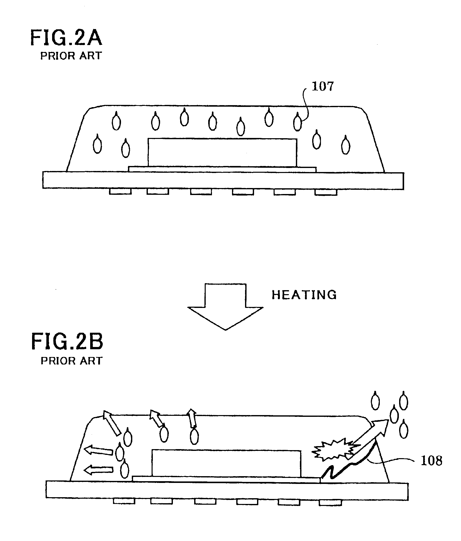
Since the molded resin 105 and such a substrate have high adhesion force with each other, it would be quite difficult for the moisture 107 to escape out of the semiconductor device 100.
However, the above-mentioned Publications cannot solve the problem mentioned earlier.

Method used


Image

  • Semiconductor device in which a semiconductor chip mounted on a printed circuit is sealed with a molded resin
  • Semiconductor device in which a semiconductor chip mounted on a printed circuit is sealed with a molded resin
  • Semiconductor device in which a semiconductor chip mounted on a printed circuit is sealed with a molded resin

Examples


first embodiment

[First Embodiment]

[0058]A resin-sealed type semiconductor device in accordance with the first embodiment is illustrated in FIGS. 3A to 3C. FIG. 3A is a top plan view of the semiconductor device, FIG. 3B is a cross-sectional view taken along the line B—B in FIG. 3A, and FIG. 3C is a cross-sectional view taken along the line C—C in FIG. 3A.

[0059]As illustrated in FIGS. 3A to 3C, the resin-sealed type semiconductor device 10 in accordance with the first embodiment is comprised of a printed wiring board 11 on which wirings are formed in a predetermined pattern, a mount 12 fixed on a surface of the printed wiring board 11, a semiconductor chip 13 fixedly mounted on the mount 12, a plurality of bonding pads 14 formed on upper and lower surfaces of the printed wiring board 11 for electrically connecting the printed wiring board 11 to an external circuit therethrough, a transparent molded-resin 15 formed on the printed wiring board 11, covering the semiconductor chip 13 therewith, and a plu...

second embodiment

[Second Embodiment]

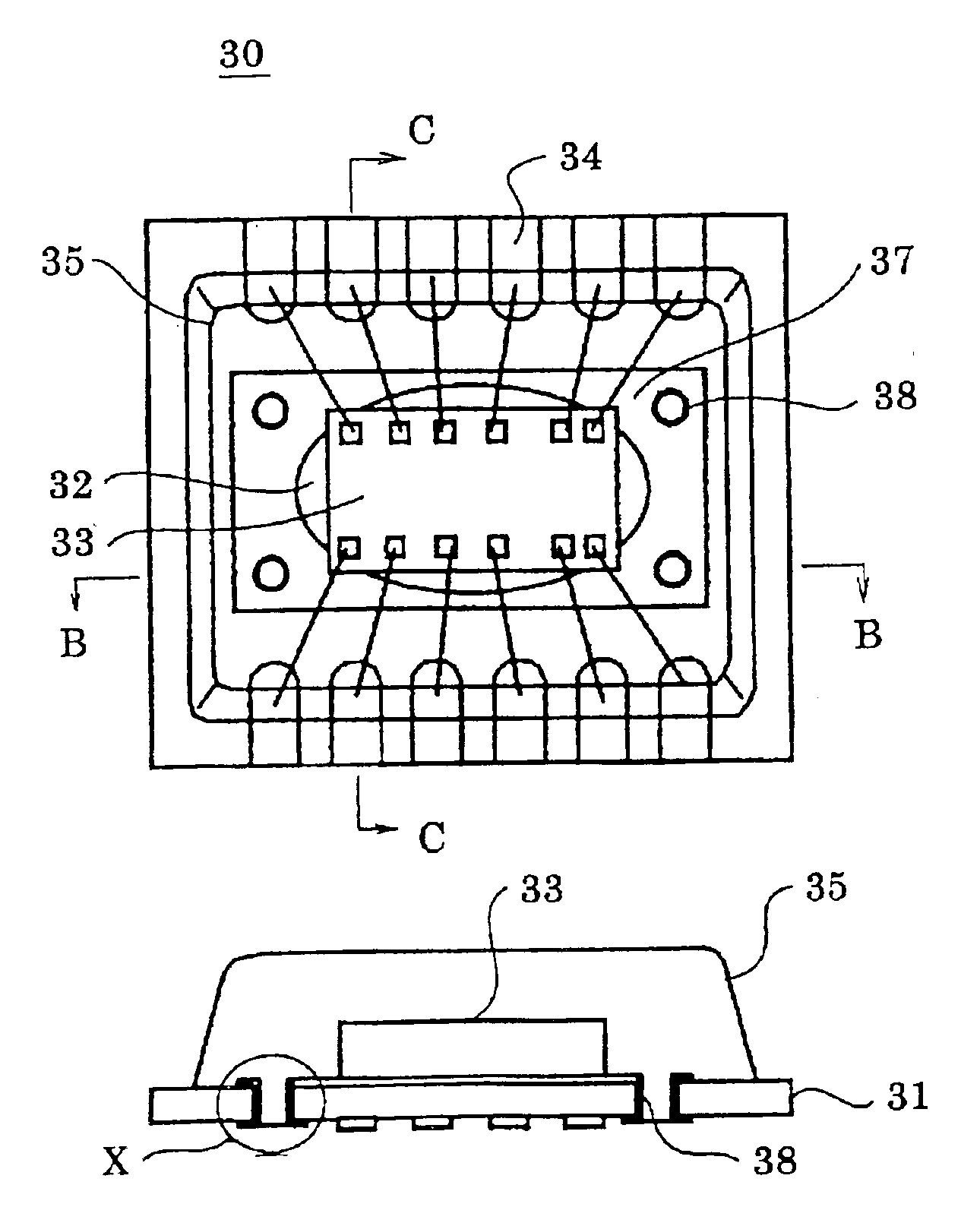
[0073]A resin-sealed type semiconductor device in accordance with the second embodiment is illustrated in FIGS. 6A to 6C and 7. FIG. 6A is a top plan view of the semiconductor device, FIG. 6B is a cross-sectional view taken along the line B—B in FIG. 6A, FIG. 6C is a cross-sectional view taken along the line C—C in FIG. 6A, and FIG. 7 is an enlarged view of an encircled portion X in FIG. 6B.

[0074]As illustrated in FIGS. 6A to 6C, the resin-sealed type semiconductor device 30 in accordance with the second embodiment is comprised of a printed wiring board 31 on which wirings are formed in a predetermined pattern, a mount 32 fixed on a surface of the printed wiring board 31, a semiconductor chip 33 fixedly mounted on the mount 32, a plurality of bonding pads 34 formed on upper and lower surfaces of the printed wiring board 31 for electrically connecting the printed wiring board 31 to an external circuit therethrough, a transparent molded-resin 35 formed on the printe...

third embodiment

[Third Embodiment]

[0083]Hereinbelow is explained a semiconductor device in accordance with the third embodiment, with reference to FIGS. 3A to 3C′.

[0084]When a metal wiring formed on a printed wiring board is plated with a metal, a solder resist 200 is first coated in a region which is not to be plated, and then, a metal wiring formed on a printed wiring board in a region where a solder resist 200 is not coated is plated with a metal. This process can be applied to the fabrication of the semiconductor device in accordance with the third embodiment.

[0085]In the semiconductor device in accordance with the third embodiment, there is intentionally formed, on the printed wiring board 11, a first region where a solder resist 200 is not to be formed, apart from a second region where a solder resist 200 is not to be coated in view of designing a wiring pattern. The first area is formed such that a metal wiring to be formed in the first area and plated with a metal extends externally beyond ...


PUM


Abstract

A semiconductor device includes (a) a printed wiring board, (b) a semiconductor chip mounted on the printed wiring board, (c) a molded resin formed on the printed wiring board, covering the semiconductor chip therewith, and (d) at least one metal wiring formed on the printed wiring board and extending externally beyond the molded resin. The metal wiring is plated with a metal having a small adhesion force with the molded resin. An interfacial surface between the metal and the molded resin acts as a path through which moisture contained in the semiconductor device escapes outside when the semiconductor device is heated.

Description

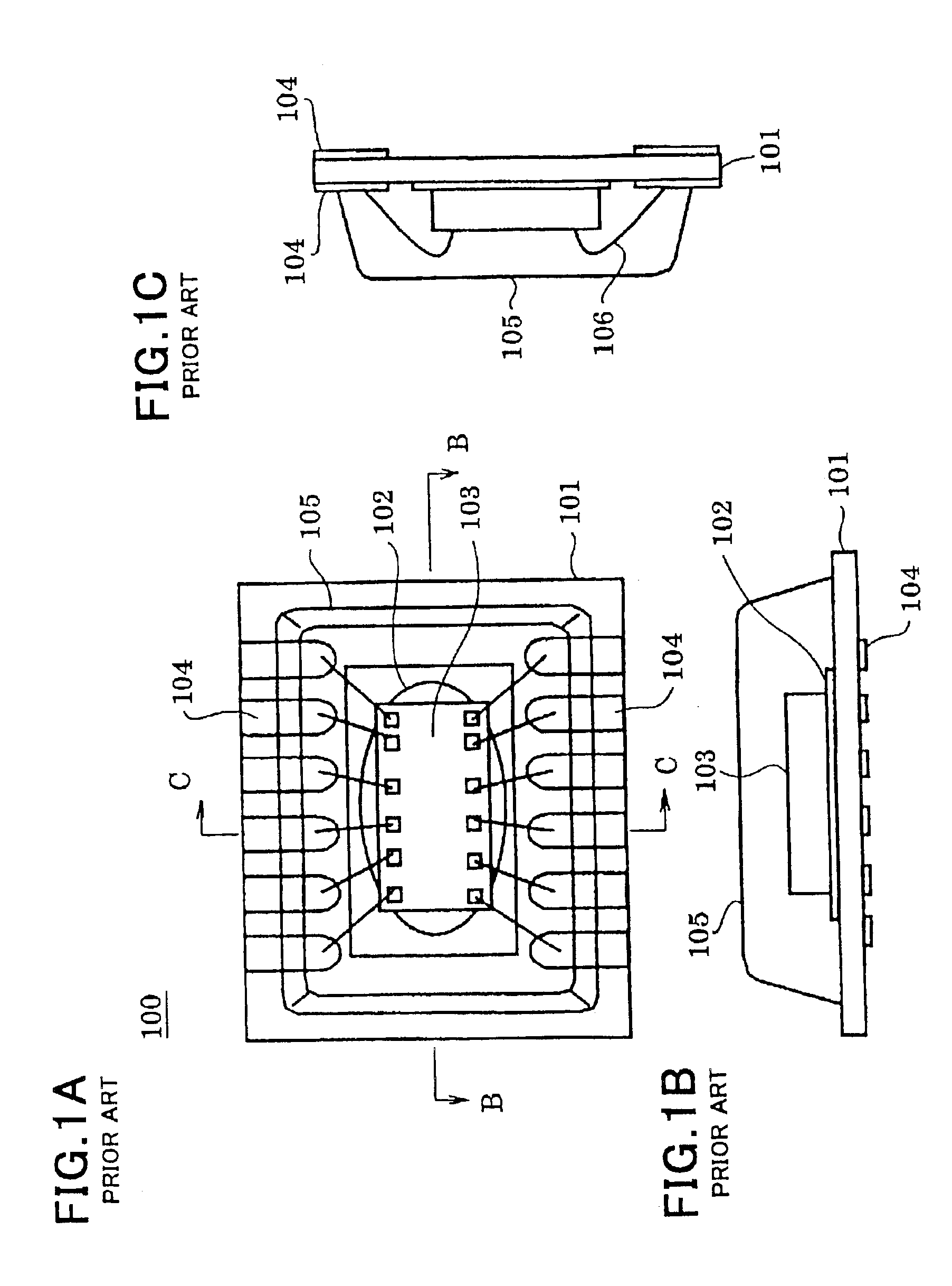
CROSS REFERENCE TO RELATED APPLICATION[0001]This Application is a divisional of U.S. application Ser. No. 10 / 202,804, filed Jul. 25, 2002.BACKGROUND OF THE INVENTION[0002]1. Field of the Invention[0003]The invention relates to a semiconductor device, and more particularly to a so-called sealed type semiconductor device in which a semiconductor chip mounted on a printed wiring board is sealed with a molded resin.[0004]2. Description of the Related Art[0005]An example of a conventional sealed type semiconductor device is illustrated in FIGS. 1A to 1C. FIG. 1A is a top plan view of a conventional sealed type semiconductor device 100, FIG. 1B is a cross-sectional view taken along the line B—B in FIG. 1A, and FIG. 1C is a cross-sectional view taken along the line C—C in FIG. 1A.[0006]As illustrated in FIGS. 1A to 1C, the conventional sealed type semiconductor device 100 is comprised of a printed wiring board 101 on which wirings are formed in a predetermined pattern, a mount 102 fixed on...

Claims


Application Information

Patent Timeline
Patent Type & Authority Patents(United States)
IPC IPC(8): H01L23/28H01L21/56H01L23/00H01L23/12H01L23/14H05K3/00H05K3/28
CPCH01L21/565H01L23/564H05K3/284H01L2224/48091H01L2224/48227H01L2224/49171H05K3/0094H01L2924/00014H01L24/48H01L24/49H01L2924/00H01L24/45H01L2224/05554H01L2224/451H01L2924/10161H01L2924/181H01L2224/45099H01L2224/05599H01L2924/00012H01L23/12
Inventor NAKAZAWA, TAIBOKIMURA, HIROYUKI
Owner RENESAS ELECTRONICS CORP
Learn More