Variable threshold semiconductor device and method of operating same

a semiconductor device and variable threshold technology, applied in the field of semiconductor devices, can solve the problems of preventing the widespread use of rtd devices in conventional silicon-based integrated circuits, -scale commercialization, and the challenge of integrating high-performance ndr devices into a conventional ic fabrication process

Inactive Publication Date: 2005-11-29
SYNOPSYS INC
View PDF50 Cites 2 Cited by
  • Summary
  • Abstract
  • Description
  • Claims
  • Application Information

AI Technical Summary

Benefits of technology

[0048]Finally, other aspects of the present invention relate to methods of making the structures and devices above. These include manufacturing processes which are compatible with conventional CMOS techniques used in commercial semiconductor facilities, thus providing a substantial advantage over the prior art. An additional benefit lies in the fact that the onset point for the negative differential resistance mode can be adjusted during the making of the device.

Problems solved by technology

To date, technological obstacles have hindered the widespread use of RTD devices in conventional silicon-based integrated circuits (ICs), however.
The most significant obstacle to large-scale commercialization has been the technological challenge of integrating high-performance NDR devices into a conventional IC fabrication process.
Efforts thus far have only yielded quantum-mechanical-tunneling-based devices that require either prohibitively expensive process technology or extremely low operating temperatures which are impractical for high-volume applications.
MBE is an expensive process which cannot be practically employed for high-volume production of semiconductor devices.
This is impractical to implement for high-volume consumer electronics applications.
A further drawback of the tunnel diode is that it is inherently a two-terminal device.
Three-terminal quantum devices which exhibit NDR characteristics such as the resonant tunneling transistor (RTT) [9] have been demonstrated; the performance of these devices has also been limited due to difficulties in fabrication, however.
Some bipolar devices (such as SCRs) also can exhibit an NDR effect, but this is limited to embodiments where the effect is achieved with two different current levels.
In other words, the I-V curve of this type of device is not extremely useful because it does not have two stable voltage states for a given current.
To date, however, the inventors are unaware of anyone succeeding with or even attempting such an approach.
Similar prior art references also identify the use of charge traps for non-volatile memories, but none again apparently recognize the potential use for such structures in an NDR context.

Method used


Image

  • Variable threshold semiconductor device and method of operating same
  • Variable threshold semiconductor device and method of operating same
  • Variable threshold semiconductor device and method of operating same

Examples


Embodiment Construction

[0053]The following detailed description is meant to be illustrative only of particular embodiments of the invention. Other embodiments of the invention and variations of those disclosed will be obvious to those skilled in the art in view of the following description.

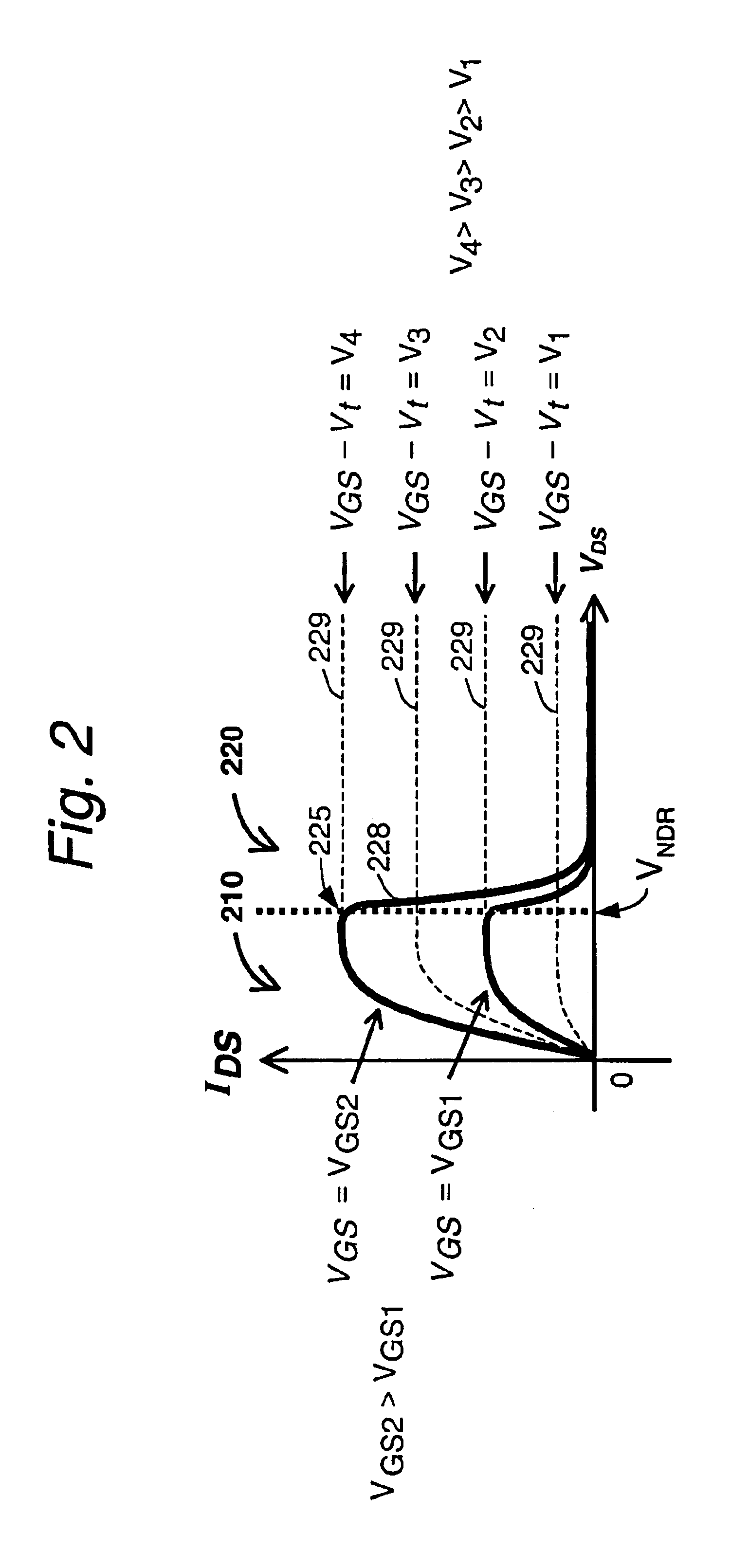
[0054]As discussed below, a preferred device embodiment is described first. Next, the mechanism responsible for the negative differential resistance (NDR) mode is described, followed by additional preferred embodiments for enhancing the performance of an NDR device. Finally, an exemplary method of fabrication will be described.

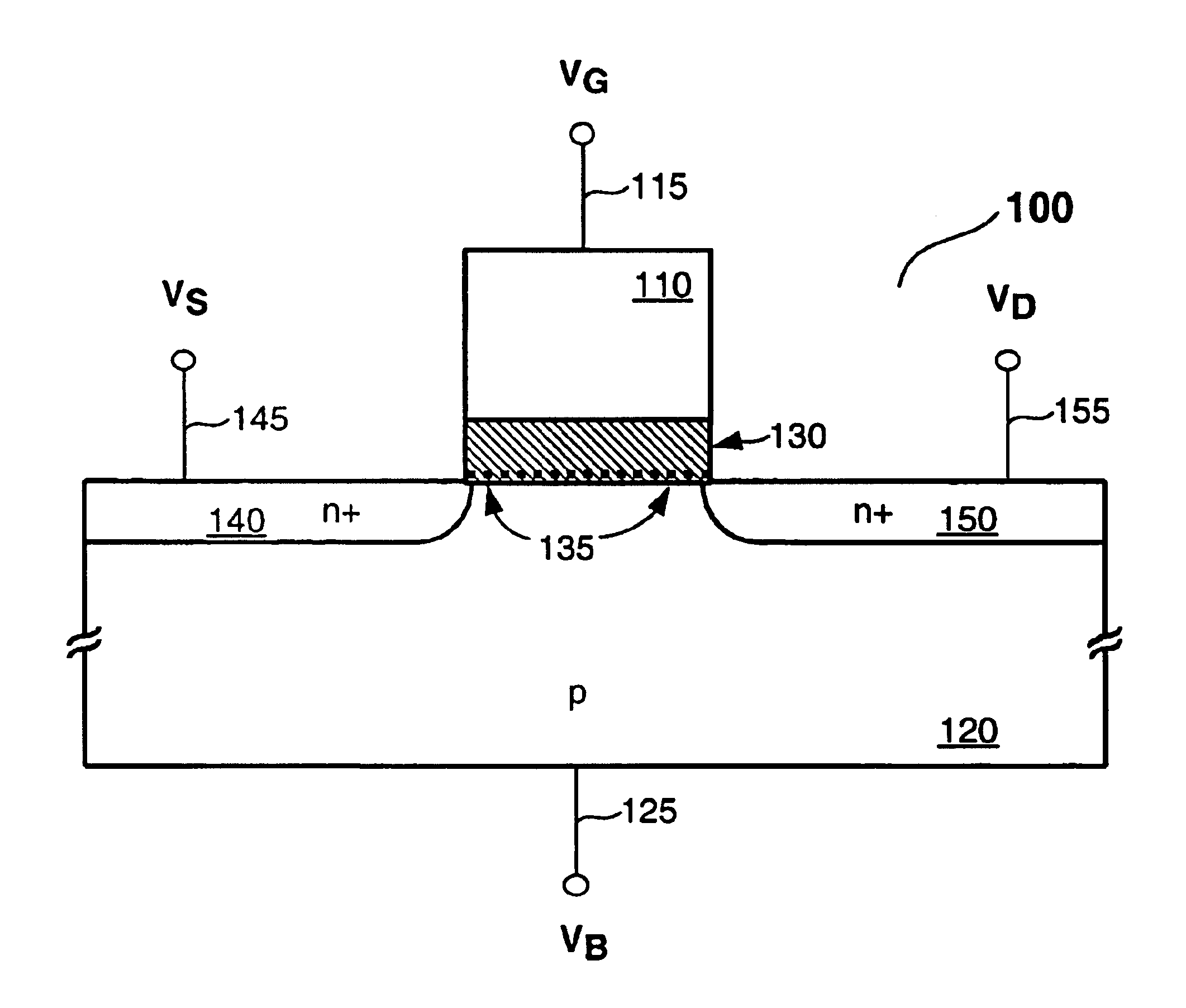
[0055]In accordance with a preferred embodiment of the invention, an n-channel MISFET NDR device structure (FIG. 1) 100 is provided which is made with minimum modification to a standard CMOS process. In fact, from a first glance, device 100 appears to be an ordinary n-channel MOS (NMOS) transistor, in which a gate electrode 110 of the device is formed on top of a semiconductor substrate 120 and el...


PUM


Abstract

An n-channel metal-insulator-semiconductor field-effect transistor (MISFET) that exhibits a variable threshold voltage is disclosed. The resulting device can be incorporated into a number of useful applications, including as part of a memory device, a logic device, etc.

Description

RELATED APPLICATIONS[0001]The present invention claims priority to and is a continuation of an application titled “CMOS PROCESS COMPATIBLE, TUNABLE NDR (NEGATIVE DIFFERENTIAL RESISTANCE) DEVICE AND METHOD OF OPERATING SAME” Ser. No. 10 / 315,741 filed Dec. 10, 2002 now U.S. Pat. No. 6,686,631. The aforementioned Ser. No. 10 / 315,741 application claims priority to and is in turn a continuation of an application titled “CMOS PROCESS COMPATIBLE, TUNABLE NDR (NEGATIVE DIFFERENTIAL RESISTANCE) DEVICE AND METHOD OF OPERATING SAME,” (Ser. No. 09 / 603,101 filed Jun. 22, 2000, now U.S. Pat. No. 6,512,274).[0002]The present application is further related to and also claims priority to an application titled “CHARGE TRAPPING DEVICE AND METHOD FOR IMPLEMENTING A TRANSISTOR HAVING A NEGATIVE DIFFERENTIAL RESISTANCE MODE” (Ser. No. 09 / 603,102 filed Jun. 22, 2000, now U.S. Pat. No. 6,479,862), and is further related to and claims priority to an application titled “CMOS COMPATIBLE PROCESS FOR MAKING A T...

Claims


Application Information

Patent Timeline
Patent Type & Authority Patents(United States)
IPC IPC(8): H01L29/78G11C5/14G11C11/39G11C16/04H01L21/28H01L21/8238H01L27/088H01L27/092H01L29/66H01L29/788H01L29/792
CPCB82Y10/00G11C5/142G11C11/39G11C16/04H01L27/088H01L29/78H01L29/788H01L29/7881H01L29/792H01L29/40114H01L29/40117
Inventor KING, TSU-JAELIU, DAVID K. Y.
Owner SYNOPSYS INC
Why Eureka
Try Eureka