Method and production of a sensor

a sensor and production method technology, applied in the field of semiconductor sensors, can solve the problems of unsuitable automation methods, unsuitable known methods, and inability to produce blocks and components which are complementary to the surface structure of the sensor surface when the block is in its operating position

Inactive Publication Date: 2005-11-15
MICRONAS
View PDF11 Cites 3 Cited by
  • Summary
  • Abstract
  • Description
  • Claims
  • Application Information

AI Technical Summary

Benefits of technology

[0011]The flowable additive material may be sprayed on the sensor in the injection molding tool. The additive material then fills the chemically ablated regions of the solidified material, which has been applied to the sensor structure or to the carrier chip as a boundary for the sensor surface. Advantageously, the same injection molding tool can be used to spray on the additive material as was used to spray on the material forming the boundary of the sensor surface. As a result, an expensive, second injection molding tool is not required.

Problems solved by technology

However, this method has a disadvantage that the block must be positioned on the sensor surface very precisely, to prevent the flowable material from penetrating between the block and the sensor surface.
A further disadvantage is that the carrier chip is damaged when the block is placed on the sensor surface, and thus the device is rendered useless or at least defective.
Another disadvantage of this method is that the production of the block and especially of the surface structure of that component which is complementary to the surface structure of the sensor surface when the block is in its operating position is still comparatively expensive.
Finally, this known method is also unsuited for automation, and thus the economical mass production of sensors.

Method used


Image

  • Method and production of a sensor
  • Method and production of a sensor
  • Method and production of a sensor

Examples


Embodiment Construction

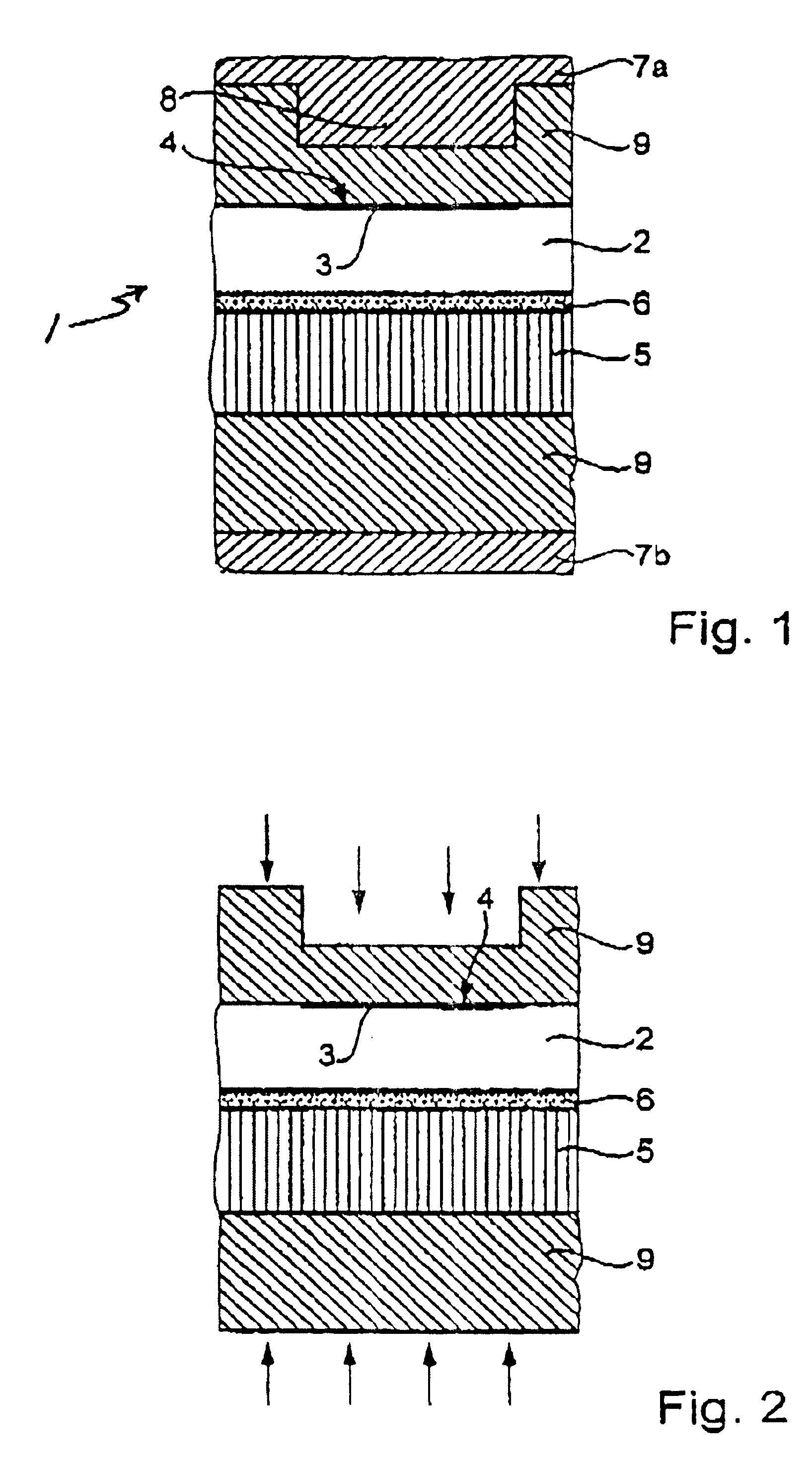
[0020]FIG. 1 shows a partial cross section through an injection molding tool, in which a semiconductor sensor chip 1 that includes an active sensor surface is situated on a frame and is encapsulated. The sensor 1 includes a carrier chip 2, which is designed as a semiconductor chip, and which has a sensor structure 3 with an active sensor surface 4. The carrier chip 2 is disposed on a frame 5, together with other carrier chips. The carrier chip 2 adheres to the frame 5 through an adhesive layer 6, which is located between the carrier chip 2 and the frame 5. The carrier chip 2, situated on the frame 5, is placed into the inner cavity of an injection molding tool, which has two molding parts 7a, 7b, that can move relative to one another and that can be brought into an open and closed position.

[0021]The injection molding tool has openings (not shown in the drawing) which are situated in the separation plane of the mold parts 7a, 7b. When the mold parts 7a, 7b are in the closed position,...


PUM


Abstract

The invention relates to a method for producing a sensor (1), wherein a carrier chip (2) is produced. Said chip is provided with a sensor structure (3) comprising an active sensor surface (4). A material (9) capable of flowing is applied onto carrier chips (2) in such a way that the sensor structure (3) has a thinner layer thickness on said active sensor surface (4) than on the area of the carrier chip (2) which borders on the active sensor surface (4). The material (9) which is capable of flowing is hardened thereafter. The hardened material (9) is subsequently removed by chemical means from the surface which faces said carrier chip (2) until the active sensor surface of the sensor structure is layed bare.

Description

BACKGROUND OF THE INVENTION[0001]The present invention relates to the field of semiconductor sensors, and in particular to a semiconductor sensor device that includes a carrier chip comprising a sensor structure with an active sensor surface, wherein a flowable material is applied to and bounds the active sensor surface region of the carrier chip, and the flowable material is then solidified.[0002]As known, for manufacturing a semiconductor sensor device, a block is first placed on the active sensor surface before flowable material is applied to the sensor chip. The outer contour of the block is matched to the outer contour of the sensor surface, so that, when the block is in its operational position, it covers only the sensor surface, while the regions surrounding the sensor surface are not covered by the block. The form of the surface structure of the block area that contacts the active sensor surface is matched to that of the active sensor surface, so the block seated on the sens...

Claims


Application Information

Patent Timeline
Patent Type & Authority Patents(United States)
IPC IPC(8): H01L21/56H01L31/0203H01L31/0232
CPCH01L21/565H01L31/0203H01L2924/0002H01L2924/00H01L31/0232
Inventor IGEL, GÜNTERROGALLA, MARKUS
Owner MICRONAS
Why Eureka
Try Eureka