Nuclear magnetic resonance equipment
a technology of nuclear magnetic resonance and equipment, applied in the direction of magnetic measurement, instruments, measurement devices, etc., can solve the problems of inability to freely choose the shape, the inability to measure for a long time, and the low intensity of the fid signal, so as to achieve the effect of higher sensitivity of the probe coil
- Summary
- Abstract
- Description
- Claims
- Application Information
AI Technical Summary
Benefits of technology
Problems solved by technology
Method used
Image
Examples
example 1
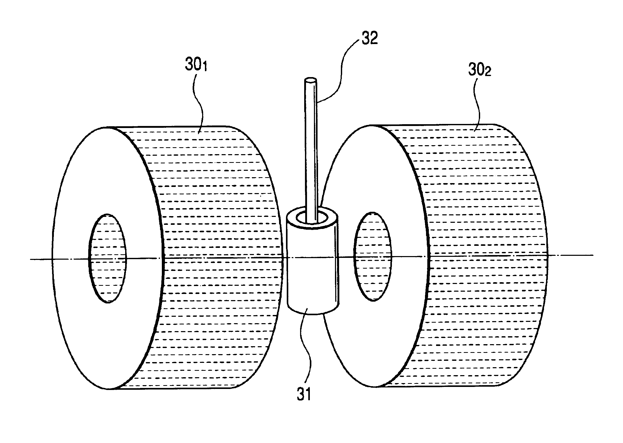
[0038]To perform NMR spectroscopy in a high frequency band exceeding 600 MHz, a structure realizing reduced inductance of a solenoid coil was examined. The solenoid coil applies a magnetic field to a sample to be measured having a diameter of 3 to 10 mm and a length of 5 to 10 mm, which is put in the sample tube 32, and for receiving a free induction decay (FID) signal. The number of turns of the coil was set to 3 or larger, and a concrete target is to achieve the capacitance of 3 pF or larger which can be realized, of a capacitor as a component of a resonator of 600 MHz.
[0039]FIG. 4 is a schematic figure of a probe coil for NMR equipment of Example 1. Like the configuration illustrated in FIG. 2, a donut plate-type coil part as a unit fabricated by a superconducting thin film formed on the donut plate-type substrate 2 (refer to FIG. 5B) and having a slit in the radial direction is basically employed. Also in FIG. 4, like FIG. 2, the donut plate-type substrate 2 is omitted and only ...
example 2
[0055]A 4-layer parallel coil was formed in the same structure as that in Example 1 except that magnesium diboride (MgB2) was changed to YBa2Cu3Oy (YBCO) as one of oxide superconductors. The donut plate-type substrate 2 was made of an La—Sr—Al—Ta oxide and the YBCO superconducting thin film 4 was formed by the pulsed laser deposition method. The same film thickness of 250 nm was used. The interlayer dielectric thin film 24 for forming the capacitor 23 between the superconducting thin film 4 and the normal metal lead 8 was formed by depositing cerium oxide (CeO2) by using a metal mask by laser vapor deposition in a manner similar to the superconducting thin film 4.
[0056]After that, the Au thin film 5 was deposited in a manner similar to Example 1 and a pattern was formed so that the superconducting thin film 4 and the Au thin film 5 overlap partially. The slit 21 and the Au thin film 5 were formed at the pitch of 15 degrees, and the thickness of the Au thin film 5 was set to 200 nm. ...
example 3
[0058]The same structure as that in Example 2 was employed except that the number of superconducting thin films was set to three. FIG. 10 is a circuit diagram showing connection. The superconducting thin film 4 used in Example 3 is a YBCO film in a manner similar to Example 1 and an LaAlO3 having a surface orientation of (001) was used for the donut plate-type substrate 2. The normal metal electrode constructing the capacitor 23 was formed by using an Ag thin film in place of the Au thin film. The thickness of the Ag thin film was 250 nm. To decrease the contact resistance between the CeO2 interlayer dielectric thin film and the Ag thin film, also in Example 3, the Ag thin film was vapor deposited and, after that, heat treatment at 400° C. for one hour was carried out in oxygen.
[0059]The fabricated 3-layer parallel coil was measured and tested at 600 MHz. As a result, though the sensitivity decreases as compared with that in the case of Example 1, the sensitivity was three times as ...
PUM
 Abstract
Description
Claims
Application Information
 - R&D
- Intellectual Property
- Life Sciences
- Materials
- Tech Scout
- Unparalleled Data Quality
- Higher Quality Content
- 60% Fewer Hallucinations
Browse by: Latest US Patents, China's latest patents, Technical Efficacy Thesaurus, Application Domain, Technology Topic, Popular Technical Reports.
© 2025 PatSnap. All rights reserved.Legal|Privacy policy|Modern Slavery Act Transparency Statement|Sitemap|About US| Contact US: help@patsnap.com


