MOSFET well biasing scheme that mitigates body effect
a well-to-substrate capacitance and biasing technology, applied in the field of biasing schemes, can solve the problems of limitation of the operation of gain-boosted operational amplifiers, physical parameters internal to these mosfets can give rise, and the overall settling behavior of operational amplifiers b>100/b> can be limited, so as to mitigate the reduction of the gain of a source follower, the effect of reducing the effect of well-to-substra
- Summary
- Abstract
- Description
- Claims
- Application Information
AI Technical Summary
Benefits of technology
Problems solved by technology
Method used
Image
Examples
first embodiment
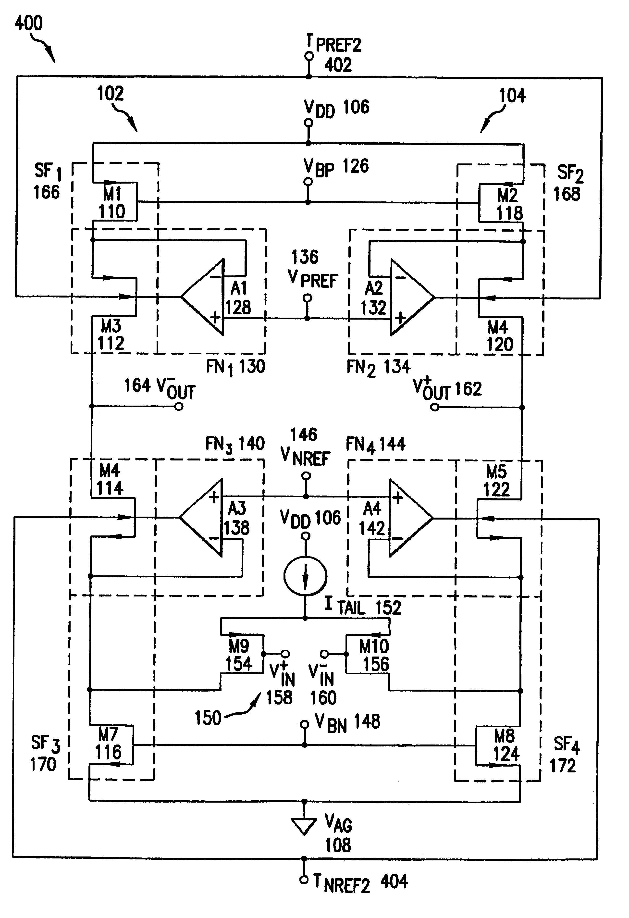
[0072]In the first embodiment, a biasing scheme is used to cause the voltage of TPREF2 402 to equal the voltage of VPREF 136. Hence, TPREF2 402 is referred to as a replica bias voltage. Because A1128 acts to maintain the voltage of the source terminal of M3112 equal to VPREF 136, the voltages of the source and body terminals of M3112 are equal. Likewise, because A2132 acts to maintain the voltage of the source terminal of M4120 equal to VPREF 136, the voltages of the source and body terminals of M4120 are equal.
second embodiment
[0073]In the second embodiment, a biasing scheme is used to cause the voltage of TNREF2 404 to equal the voltage of VNREF 146. Hence, TNREF2 404 is referred to as a replica bias voltage. Because A3138 acts to maintain the voltage of the source terminal of M5114 equal to VNREF 146, the voltages of the source and body terminals of M5114 are equal. Likewise, because A4142 acts to maintain the voltage of the source terminal of M6122 equal to VNREF 146, the voltages of the source and body terminals of M6122 are equal.
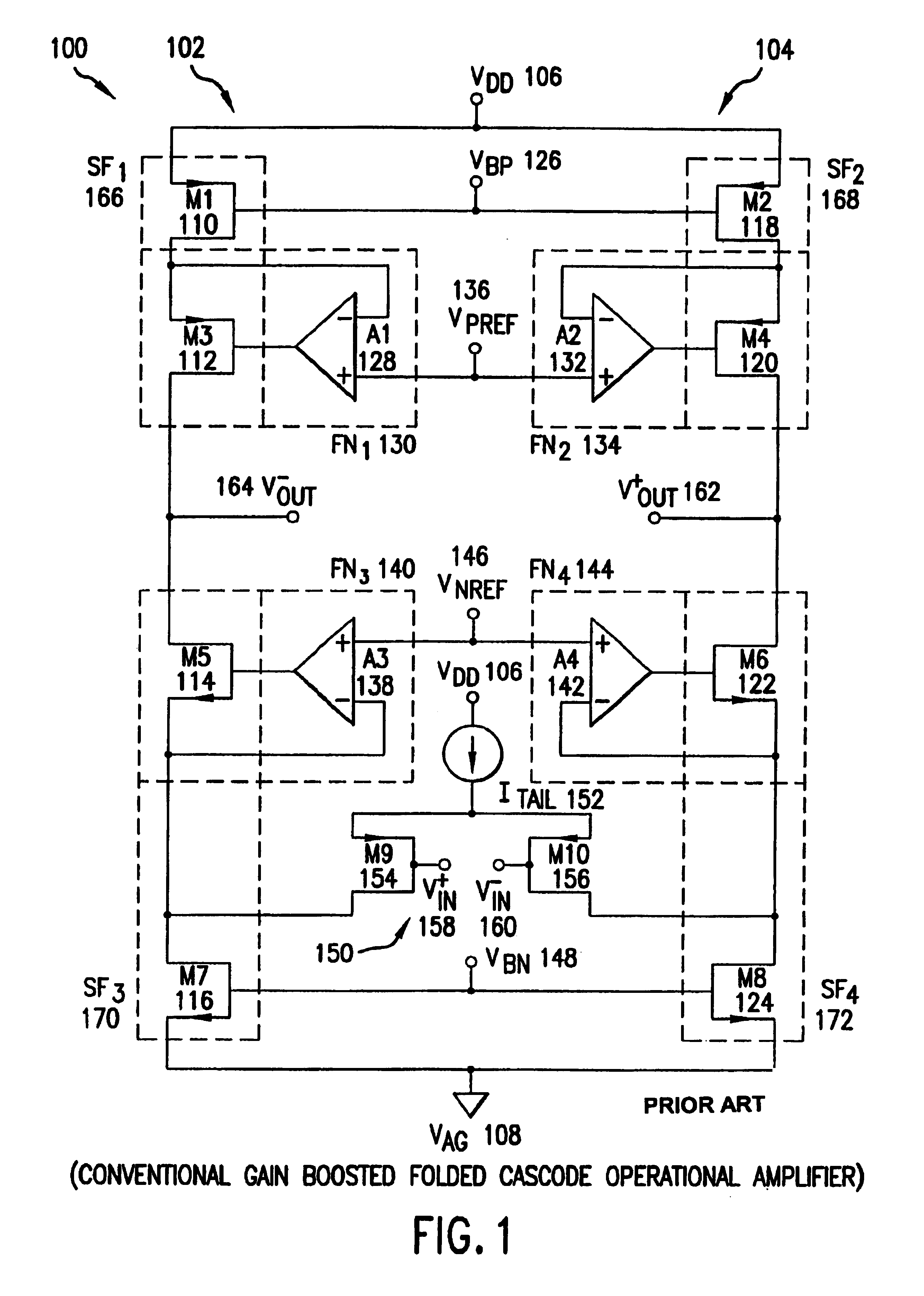
[0074]Thus, for each driven MOSFET (e.g., M3112, M4120, M5114, or M6122), the biasing scheme makes VSB equals zero. On its face, by application of Eq. (9), the effect of having VSB equal to zero appears to increase the value of the body transconductance gmb. Hence, by application of Eq. (8), this appears to reduce the gain A of the corresponding source follower (e.g., SF1 166, SF2 168, SF3 170, or SF4 172), which, by application of Eq. (6), appears to increase the capacitive...
embodiment 1000
[0105]FIG. 10A is a schematic diagram of an embodiment 1000 of the present invention to bias a MOSFET 1002. In FIG. 10A, the source terminal of MOSFET 1002 is connected to the noninverting terminal of an operational amplifier 1004. The output of operational amplifier 1004 is applied both to its inverting terminal and to the body terminal of MOSFET 1002. Because operational amplifier 1004 acts to make the voltages at it inverting and noninverting terminals equal, and because the voltage at the inverting terminal is equal to the voltage at the output, operational amplifier 1004 comprises a circuit that replicates the voltage at the source terminal of MOSFET 1002 and applies this replicated voltage to the body terminal of MOSFET 1002.
[0106]FIG. 10B is a schematic diagram of an alternative embodiment 1006 of the present invention to bias MOSFET 1002. In FIG. 10B, MOSFET 1002 is connected between a first current source “I1”1008 and VAG 108. A second MOSFET 1010 is connected between a sec...
PUM
 Abstract
Description
Claims
Application Information
 - R&D
- Intellectual Property
- Life Sciences
- Materials
- Tech Scout
- Unparalleled Data Quality
- Higher Quality Content
- 60% Fewer Hallucinations
Browse by: Latest US Patents, China's latest patents, Technical Efficacy Thesaurus, Application Domain, Technology Topic, Popular Technical Reports.
© 2025 PatSnap. All rights reserved.Legal|Privacy policy|Modern Slavery Act Transparency Statement|Sitemap|About US| Contact US: help@patsnap.com


