Semiconductor memory device having the operating voltage of the memory cell controlled
a memory device and integrated circuit technology, applied in the direction of information storage, static storage, digital storage, etc., can solve the problems of inability to operate the circuit, the operation margin of not only reading but also writing becomes smaller, and the sram circuit cannot opera
- Summary
- Abstract
- Description
- Claims
- Application Information
AI Technical Summary
Benefits of technology
Problems solved by technology
Method used
Image


Examples
embodiment 1
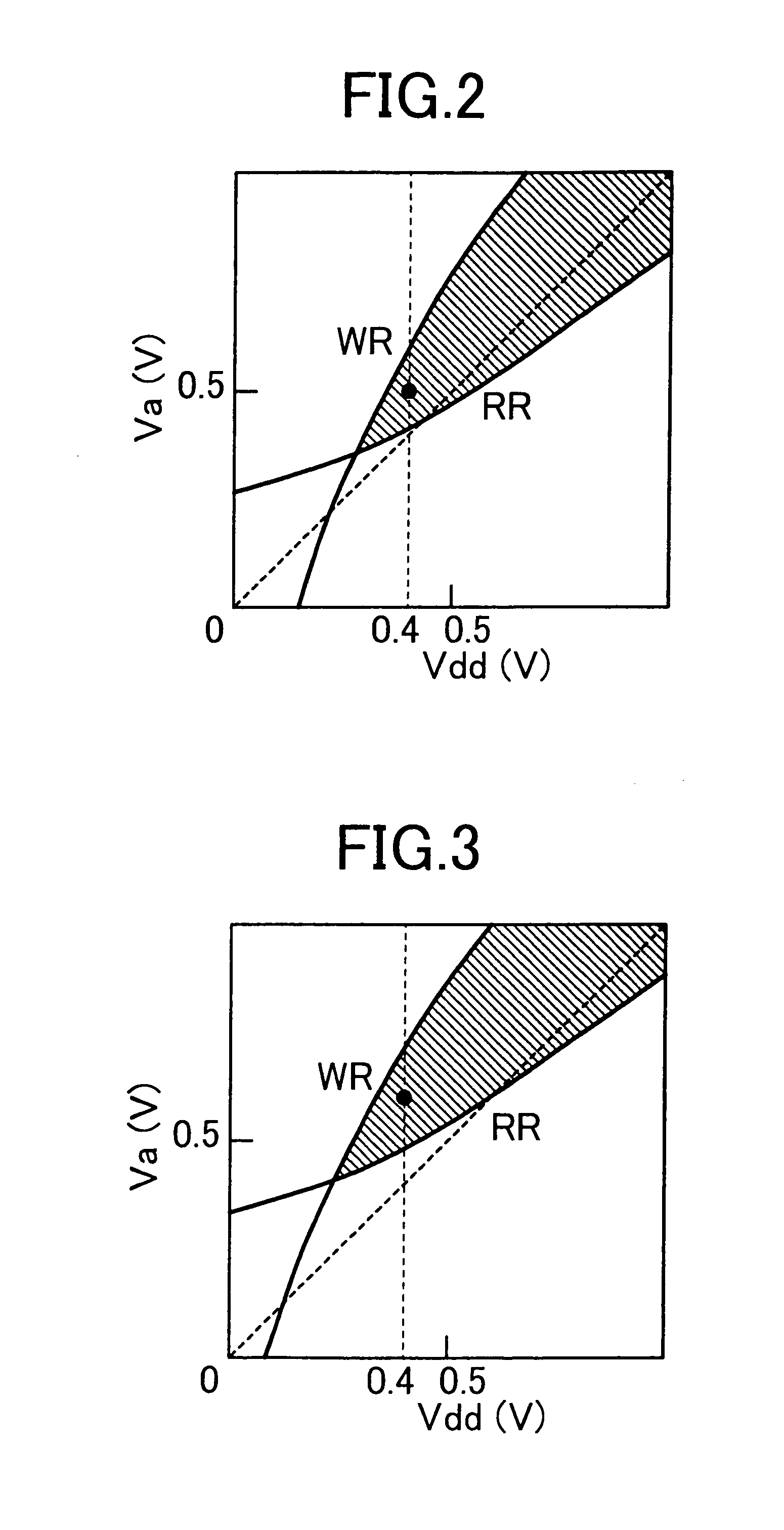
[0023]FIG. 1 schematically shows a SRAM circuit and its power constitution according to the present invention. In FIG. 1, MA is an array of SRAM memory cells, WD is a circuit for controlling the word line, a word driver or a row address decoder, SA is a circuit for controlling the bit line, a sense amplifier, precharging circuit or column decoder, DTVT1 is a circuit which detects the threshold voltage of pMOS and nMOS transistors and generates reference potential signal sigref1 for generating the operating operating voltage of the memory array, and CTVA is a power circuit for outputting an operating voltage Va of the memory array by increasing or reducing the operating voltage Vdd based on the signal sigref1 from DTVT1. Wl in the memory array MA is the word line of a memory cell, bl and blb are bit lines, Vss is a ground potential line, Vbp is a node connected to the substrate electrode of a pMOS transistor in the memory cell, and Vbn is a node connected to the substrate electrode o...
embodiment 2
[0031]FIG. 7 schematically shows another SRAM circuit and its voltage control constitution. In FIG. 7, MA is an array of SRAM memory cells, WD is a circuit for controlling the word line, a word driver, and row address decoder, SA is a circuit for controlling the bit line, a sense amplifier, precharger circuit and column decoder, BOOST 2 is a booster circuit for increasing Vdd to generate voltage Vddu, CTVA is a voltage controlling circuit for outputting an operating voltage Va for the memory array based on a reference potential signal sigref2, DREG1 is a circuit for outputting a reference potential specified by a reference potential selection signal swcont1, and DTVT2 is a circuit for outputting a reference potential selection signal swcont1 in accordance with the threshold voltages of transistors. During the operation of this circuit, the threshold voltage detection circuit DTVT2 outputs a signal swcont1 for selecting the optimum voltage for the memory array based on the threshold ...
embodiment 3
[0037]FIG. 11 schematically shows still another SRAM circuit according to the present invention. In FIG. 11, MA is an array of SRAM memory cells, WD is a circuit for controlling the word line, a word driver, row address decoder, SA is a circuit for controlling the bit line, a sense amplifier, precharger circuit and column decoder, DTVT3 is a circuit for detecting the threshold voltages of transistors and generating a reference potential signal sigref3 for generating an operating voltage for the memory array and reference potential signals sigref4 and sigref5 for generating substrate potentials for the memory array, CTVA is a voltage control circuit for increasing or reducing the operating voltage Vdd based on the signal sigref3 from DTVT3 to apply an operating voltage Va to the memory array, and CTVBB is a circuit for generating Vbn and Vbp which are substrate potentials for the memory array in response to the signals sigref4 and sigref5 from DTVT3. Vbn is a potential for p well whi...
PUM
 Abstract
Description
Claims
Application Information
 - R&D
- Intellectual Property
- Life Sciences
- Materials
- Tech Scout
- Unparalleled Data Quality
- Higher Quality Content
- 60% Fewer Hallucinations
Browse by: Latest US Patents, China's latest patents, Technical Efficacy Thesaurus, Application Domain, Technology Topic, Popular Technical Reports.
© 2025 PatSnap. All rights reserved.Legal|Privacy policy|Modern Slavery Act Transparency Statement|Sitemap|About US| Contact US: help@patsnap.com