Supercharge Your Innovation With Domain-Expert AI Agents!
Semiconductor device and its manufacturing method
Inactive Publication Date: 2005-10-11
RENESAS NORTHERN JAPAN SEMICON +1
View PDF9 Cites 3 Cited by
Summary
Abstract
Description
Claims
Application Information
AI Technical Summary
This helps you quickly interpret patents by identifying the three key elements:
Problems solved by technology
Method used
Benefits of technology
Benefits of technology
[0036]According to the above means (1) there accrue the following advantages.
[0043](g) Since the insulating base layer is formed by a flexible resin film and its thickness is about 30 to 100 μm, the stress after the mounting of the semiconductor device onto the packaging substrate is relaxed and the packaging reliability is enhanced.
Problems solved by technology
The above flip chip packaging methods give rise to the following problems.
Therefore, in the above method (1) wherein bump electrodes are formed directly on the peripheral electrodes of the semiconductor chip, the pitch of the bump electrodes thus formed is small and it is accordingly required to use a build-up type packaging substrate which is more expensive than the ordinary type of packaging substrates.
However, since the manufacturing process is applied, including defective ships in a state of wafer, an increase of cost results, and it is difficult to form a mechanism for relaxing a thermal stress which is induced between the packaging substrate and the semiconductor chip in the foregoing WPP method.
However, the build-up method is more complicated in the manufacturing process than the laminate method and the resulting substrate is 1.7 to 2 times more expensive than the substrate obtained by the laminate method.
Method used
Image
Click on the blue label to locate the original text in one second.
Reading with bidirectional positioning of images and text.
Examples
first embodiment
(First Embodiment)
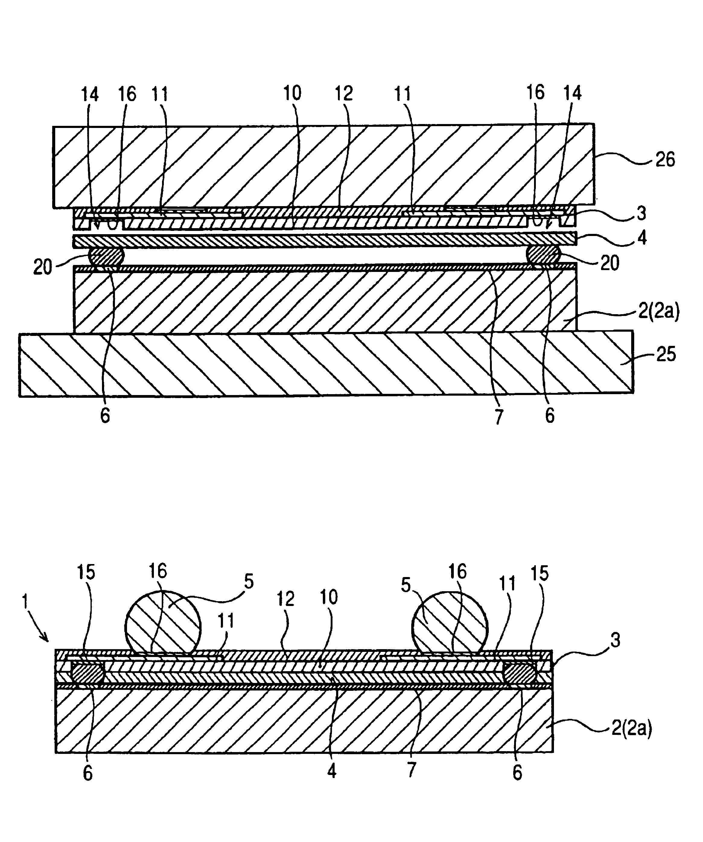
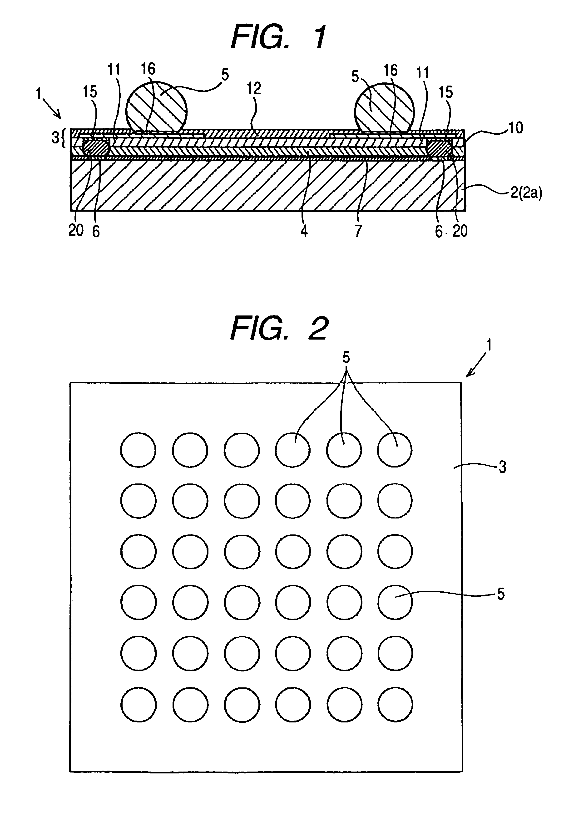
[0070]FIGS. 1 to 14 are concerned with a semiconductor device according to one embodiment (first embodiment) of the present invention, of which FIG. 1 is a schematic sectional view of the semiconductor device, FIG. 2 is a plan view thereof, FIG. 3 is a back view thereof, and FIG. 4 is a schematic plan view of the semiconductor device, showing a state of connection between area array bump electrodes and electrodes of a semiconductor chip.
[0071]As shown in FIG. 1, the semiconductor device of this first embodiment, indicated at 1, is of a structure wherein a wiring substrate (wiring tape substrate) 3 is stacked and bonded onto a main surface (upper surface in FIG. 1) of a semiconductor chip 2 through an adhesive 4, and solder salient electrodes (area array bump electrodes) 5 are formed on an exposed surface (upper surface in FIG. 1) of the wiring tape substrate 3.
[0072]In FIG. 1, two area array bump electrodes 5 are shown in an enlarged and schematic manner also for m...
third embodiment
(Third Embodiment)
[0110]FIG. 16 is a schematic sectional view showing a semiconductor device according to a further embodiment (third embodiment) of the present invention. In this third embodiment, wiring lines in a wiring tape substrate 3 are formed in multiple layers to increase the degree of margin for wiring distribution.
[0111]More specifically, in the semiconductor device 1 of the first embodiment, one interlayer insulating film 40 of a predetermined pattern is formed on the wiring lines 11 formed on the surface of the tape base 10, then wiring lines 11a are formed on the interlayer insulating film 40 and are covered with the solder resist 12 which is formed selectively, further, there are formed area array bump electrodes 5 connected electrically to the wiring lines 11a.
[0112]The wiring lines 11 connected electrically to the gold wire bump electrodes 20 formed on the electrodes 6 of the semiconductor chip 2 and the area array bump electrodes 5 formed on the surface of the tap...
fourth embodiment
(Fourth Embodiment)
[0118]FIG. 17 is a schematic sectional view showing a semiconductor device according to a still further embodiment (fourth embodiment) of the present invention. According to this fourth embodiment, the pitch of area array bump electrodes 5 can be made wider.
[0119]More specifically, in this fourth embodiment, the wiring tape substrate 3 in the semiconductor device of the first embodiment is made larger (larger in area) than the semiconductor chip 2, as shown in FIG. 17. According to the structure of this fourth embodiment, the outer periphery of the wiring tape substrate 3 is projected from all the peripheral edges of the semiconductor chip 2.
[0120]In this embodiment, since the wiring tape substrate 3 can be made wide, the pitch of the area array bump electrodes 5 can be made larger than that in the first embodiment and hence it is possible to set large the pitch of electrodes on the packaging substrate for packaging the semiconductor device of this embodiment.
PUM
Property
Measurement
Unit
Elastic modulus
aaaaa
aaaaa
aaaaa
aaaaa
Abstract
A semiconductor device having area array bump electrodes suitable for flip chip packaging is disclosed. A semiconductorchip with wire bonding electrodes arranged along peripheral edges thereof is provided, then gold wire bump electrodes are formed over the wire bonding electrodes, and thereafter a wiring tape substrate is superimposed on the semiconductorchip and is bonded thereto with an adhesive. On a back surface of the wiring tape substrate are formed wiring connections correspondingly to the electrodes. Further, at the time of bonding with use of the adhesive, convex tips of the gold wire bump electrodes formed respectively on the electrodes of the semiconductor chip pierce through the adhesive to connect the gold wire bump electrodes and the connections electrically with each other. On a surface of the wiring tape substrate are formed area array bump electrodes, whose pitch is larger than the pitch of the electrodes formed on the semiconductor chip.
Description
FIELD OF ART[0001]The present invention relates to a semiconductor device and a method of manufacturing the same. Particularly, the present invention is concerned with a technique which can convert a semiconductor chip having wire bonding electrodes on a surface thereof into a semiconductor device having area array bump electrodes capable of being flip chip packaged.BACKGROUND ART[0002]Recently, in electronic devices with a semiconductor device incorporated therein, not only there has been a tendency to high speed, high function, and high packaging density, but also efforts have been made for the reduction of thickness and weight. Particularly, flip chip packaging of a semiconductor chip (semiconductor element) with LSI, etc. incorporated therein is effective for the attainment of high speed and thickness reduction.[0003]Flip chip packaging methods are broadly classified into the following two methods. (1) Gold stud bumps are formed on peripheral electrodes (e.g., aluminum electrode...
Claims
Application Information
Patent Timeline
Application Date:The date an application was filed.
Publication Date:The date a patent or application was officially published.
First Publication Date:The earliest publication date of a patent with the same application number.
Issue Date:Publication date of the patent grant document.
PCT Entry Date:The Entry date of PCT National Phase.
Estimated Expiry Date:The statutory expiry date of a patent right according to the Patent Law, and it is the longest term of protection that the patent right can achieve without the termination of the patent right due to other reasons(Term extension factor has been taken into account ).
Invalid Date:Actual expiry date is based on effective date or publication date of legal transaction data of invalid patent.
