
Methods for making reinforced wafer polishing pads and apparatuses implementing the same

a technology of reinforced wafers and polishing pads, which is applied in the direction of manufacturing tools, grinding devices, lapping machines, etc., can solve the problems of prior art designs having serious delamination problems, the delamination of the polishing belt is significantly more difficult, and the manufacturing of further metallization layers becomes substantially more difficult, so as to achieve more repeatability, improve efficiency and effective polishing operations

Inactive Publication Date: 2005-09-27
LAM RES CORP
View PDF7 Cites 13 Cited by
  • Summary
  • Abstract
  • Description
  • Claims
  • Application Information

AI Technical Summary

Benefits of technology

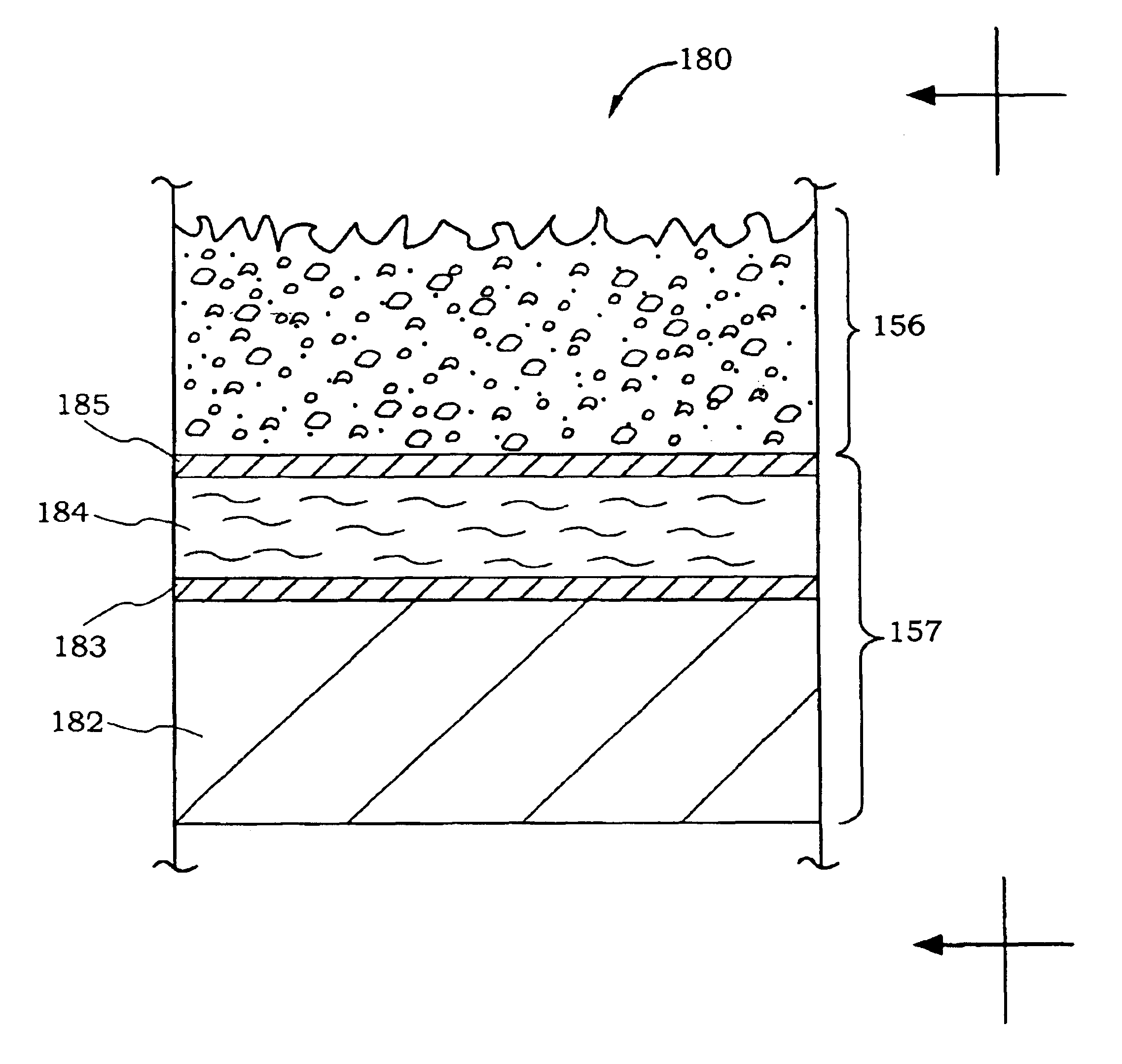
[0026]The advantages of the present invention are numerous. Most notably, by constructing a polishing pad and supporting structure in accordance with any one of the embodiments of the present invention, the polishing pad and supporting structure will be able to provide more efficient and effective polishing operations over wafer surfaces (e.g., metal and oxide surfaces). Furthermore, because the wafers placed through a CMP operation using the improved polishing pad are polished with better repeatability and more consistency, the CMP operation will also result in improved wafer yields. The polishing structure of the present invention may be strongly held together by dynamically cured adhesives and / or fusing. Therefore the polishing structure may resist shearing forces much better than the prior art thus greatly decreasing the possibility of polishing pad delamination. In addition, because the polishing pad does not have seams, it will be more resistant to delamination than the prior art. Still further, due to the increased resistance to delamination, the polishing pad of the present invention lasts longer and may have to be changed much less frequently. Consequently, due to the substantial increase in the polishing pad life, the CMP operations have to be stopped less frequently to change the polishing pad. Because of the time often necessary to change polishing pads in prior art belt polishing systems, the significantly more durable polishing pad structure of the present invention may result in a significantly increased wafer production. Other aspects and advantages of the present invention will become apparent from the following detailed description, taken in conjunction with the accompanying drawings, illustrating by way of example the principles of the present invention.

Problems solved by technology

Without planarization, fabrication of further metallization layers becomes substantially more difficult due to the variations in the surface topography.
The moisture may then attack the adhesive holding the polishing belt and the supporting layer together thus causing delamination of the polishing belt from the supporting layer.
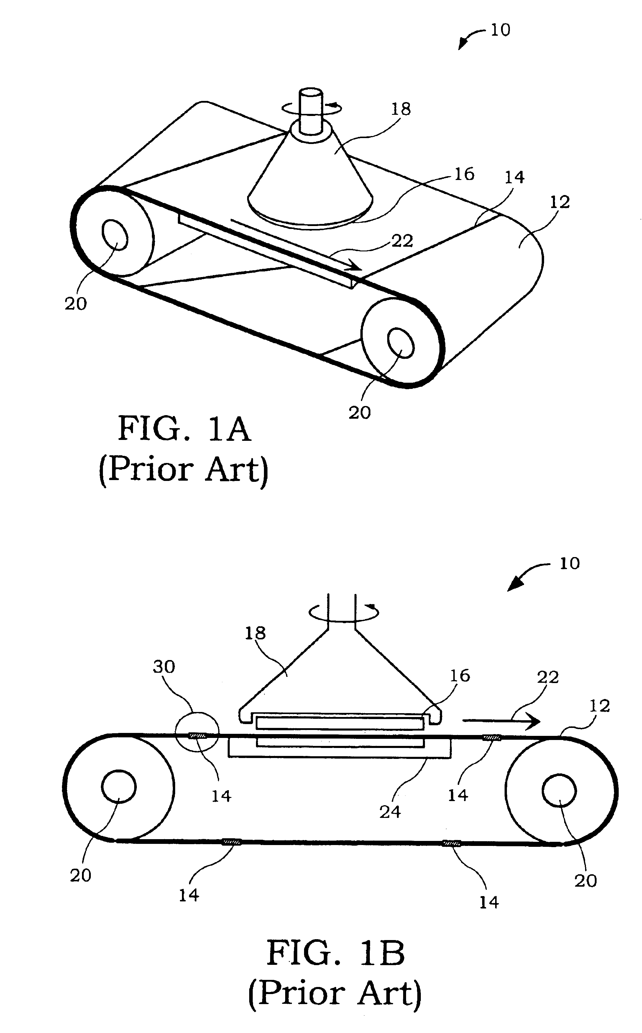
Therefore, the prior art designs have serious delamination problems due to moisture intrusion into the seams 14.
In addition, shear forces created between the support layer and the polishing belt 12 when moving over the rollers 20 can be a very serious destructive factor and also cause delamination.
As a result, the life of the polishing belt may be shortened significantly.
Such a shortening of polishing belt life may then cause a considerable decrease in wafer production.
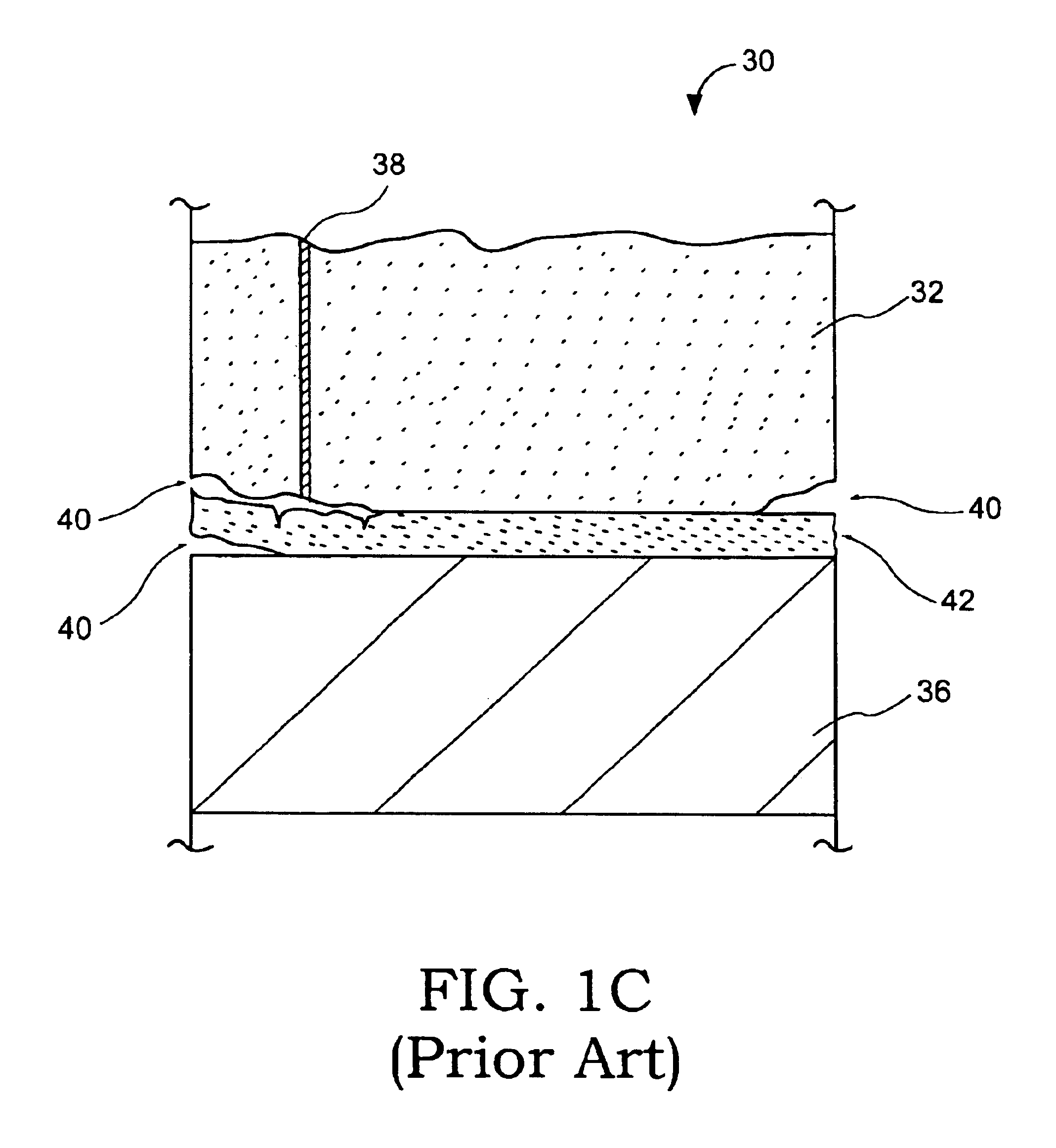
1C), shear forces may be created causing serious delaminatory damage.
This shear stress may lead to delamination over time.
The delaminations 40 tend to destabilize the polishing pad and significantly reduce the effectiveness and life of the polishing pad.
As a result, the polishing pad of the prior art has a reduced life span and therefore wafer production throughput may be drastically reduced due to the time necessary to change the polishing pad.
The reduced lifetime of polishing pads also results in the use of more polishing pads by a manufacturer thus incurring even more costs.
In addition, if unanticipated delaminations occur, wafers polished by delaminated polishing belts may be defective thus creating further costs for a wafer manufacturer.
As indicated previously, changing pads on a polishing belt may be an extremely expensive and time consuming process.
This can cause a long period of wafer processing shutdown and can potentially decrease wafer production severely.
Therefore, polishing belt structure which breaks down and delaminates after a short period of time may create extreme problems for entities requiring constant and consistent wafer production.
Unfortunately the prior art method and apparatus of CMP operations as described in reference to FIGS. 1A, 1B, and 1C have even more problems.
The prior art apparatus also has problems with oxide removal where the topographical nature of the wafers include varying thickness of metallic and dielectric layers such as those found when gaps are formed during the application of such layers.
Again, these prior art difficulties arise due to the inability to properly control the polishing pressure applied to the wafer surface due to the lack of cushioning of the polishing pad.
Consequently, these problems arise due to the fact that the prior art polishing belt designs do not properly control polishing dynamics because of the lack of cushioning in the polishing pad.

Method used


Image

  • Methods for making reinforced wafer polishing pads and apparatuses implementing the same
  • Methods for making reinforced wafer polishing pads and apparatuses implementing the same
  • Methods for making reinforced wafer polishing pads and apparatuses implementing the same

Examples


Embodiment Construction

[0042]An invention for a method of making a polishing pad structure and an apparatus using the same is disclosed. In the following description, numerous specific details are set forth in order to provide a thorough understanding of the present invention. It will be understood, however, by one of ordinary skill in the art, that the present invention may be practiced without some or all of these specific details. In other instances, well known process operations have not been described in detail in order not to unnecessarily obscure the present invention.

[0043]In general terms, the present invention is directed toward a polishing pad structure and method for making the structure. The polishing pad structure includes a supporting layer, a cushioning layer, and a pad layer. In a preferred embodiment, the pad layer is designed and made as a contiguous and seamless unit, and is preferably adhered to the cushioning layer to enable more consistent and effective wafer polishing during CMP op...


PUM


Abstract

As one of many embodiments of the present invention, a seamless polishing apparatus for utilization in chemical mechanical polishing is provided. The seamless polishing apparatus includes a polishing pad where the polishing pad is shaped like a belt and has no seams. The seamless polishing apparatus also includes a base belt where the base belt includes a reinforcement layer where the reinforcement layer is a fibrous-type material. In addition, the polishing pad is located over the base belt.

Description

CROSS REFERENCE TO RELATED APPLICATIONS[0001]This is a continuation application of U.S. patent application Ser. No. 09 / 752,509, filed on Dec. 27, 2000, now U.S. Pat. No. 6,561,889, entitled “METHODS FOR MAKING REINFORCED WAFER POLISHING PADS AND APPARATUSES IMPLEMENTING THE SAME” from which priority under 35 U.S.C. §120 is claimed. The aforementioned patent application is hereby incorporated by reference in its entirety. This application is a also related to U.S. patent application Ser. No. 09 / 752,703, filed on Dec. 27, 2000, entitled “METHODS FOR MAKING REINFORCED WAFER POLISHING PADS UTILIZING DIRECT CASTING AND APPARATUSES IMPLEMENTING THE SAME.”BACKGROUND OF THE INVENTION[0002]1. Field of the Invention[0003]The present invention relates to chemical mechanical polishing (CMP) techniques and, more particularly, to the efficient, cost effective, and improved CMP operations.[0004]2. Description of the Related Art[0005]In the fabrication of semiconductor devices, there is a need to p...

Claims


Application Information

Patent Timeline
IPC IPC(8): B24D18/00B24B37/04B24D11/00B24B37/22B24B37/24
CPCB24B37/22B24B37/24B24D18/0009
Inventor XU, CANGSHANZHAO, EUGENE Y.DAI, FEN
Owner LAM RES CORP
Learn More