
Apparatus and method for detecting photon emissions from transistors

a transistor and photon emission technology, applied in the direction of electronic circuit testing, measurement devices, instruments, etc., can solve the problems of difficult or impossible to physically test such small discrete elements of an ic, poor quantum efficiency of the available pmt detectors in the near infrared spectrum, and difficult to perform physical probing of the ic. easy to achieve the effect of reducing the time required, rapidly detecting the difference between photons emitted, and rapid extraction of transistor timing information

Inactive Publication Date: 2005-09-13
DCG SYST
View PDF58 Cites 19 Cited by
  • Summary
  • Abstract
  • Description
  • Claims
  • Application Information

AI Technical Summary

Benefits of technology

[0013]Aspects of the present invention dramatically reduce the time required to acquire a sufficient number of transistor emitted photons to extract useful information. Implementations of the present invention can be used to rapidly discriminate between photons emitted from transistors and background photon emissions. Implementations of the present invention may also be used to rapidly extract transistor timing information. In some instances, data acquisition times can be reduced from several hours or days, to only several minutes. With such reductions in acquisition time, emission data from an entire IC may be obtained in the time it would take to obtain data for only a single discrete area of an IC, and probe systems may be used to acquire data for numerous ICs in the time it would take to acquire data for a single IC. By shortening the time for testing and debugging of ICs, chip makers can bring new products to market faster than with conventional probe systems, can identify and rectify faults faster than with conventional probe systems, and can realize numerous other advantages.
[0014]Implementations of the present invention also automatically identify transistors from photon emission data. Upon automatic identification of transistors, histograms for all identified transistors may be automatically generated. This eliminates the need for a user to visually determine which photon data might be from a transistor, manually select the photon emission data, and then generate a histogram. Moreover, the number of photons required to obtain highly accurate transistor timing information is dramatically reduced.
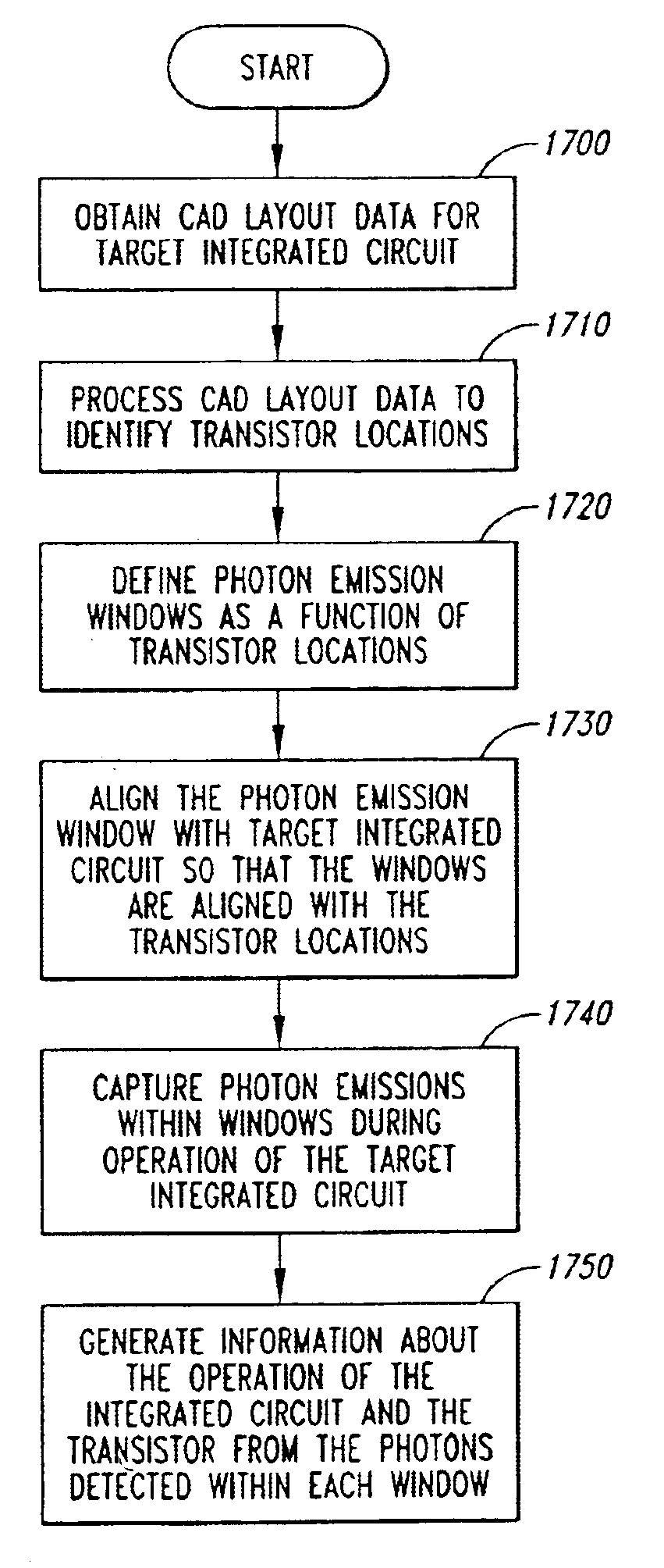
[0025]Yet another aspect of the invention involves a method for reducing diagnostic time of a photon detecting integrated circuit tester. At one level, the method involves processing a CAD database associated with an integrated circuit and defining at least one CAD layer from the CAD database, the at least one CAD layer identifying at least one expected photon emission source of the integrated circuit. The method may further comprises the operation of aligning the tester with the at least one CAD layer to correlate the tester with the at least one expected photon emission source. The method may also further comprise identifying photon emissions from the at least one expected photon emission source, the photon emissions detected by the tester during operation of the integrated circuit.

Problems solved by technology

Testing such small discrete elements of an IC is difficult or impossible to perform by physically probing the IC.
Moreover, physically probing the IC can easily damage it.
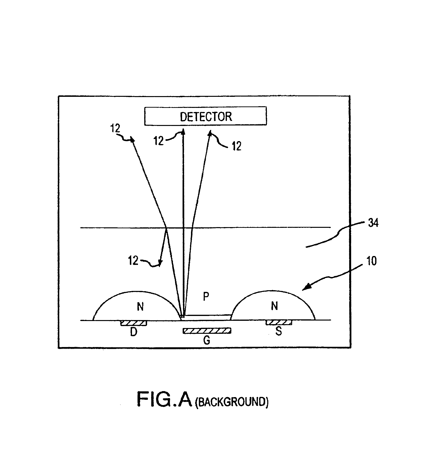
The quantum efficiency of the available PMT detectors is poor in the near infrared spectrum, but is higher in the visible spectrum.
The detection of 10 million or more photons may take hours or days, which in some instances may be prohibitively long.
One drawback of conventional probe systems is that they lack the ability to process the photon emission data to automatically identify photons that were emitted by transistors.
Thus, while conventional probe systems provide extremely useful testing information, the time required to obtain that information can be very long.

Method used


Image

  • Apparatus and method for detecting photon emissions from transistors
  • Apparatus and method for detecting photon emissions from transistors
  • Apparatus and method for detecting photon emissions from transistors

Examples


Embodiment Construction

[0083]The present invention involves apparatuses and methods for analyzing photon emissions from an integrated circuit (IC) to identify transistors and extract timing information. Implementations of the present invention process photon emission data to rapidly discriminate between photons emitted by a transistor and photons attributable to background emissions. Generally, various aspects of the invention involve the correlation, grouping, or association of photons that have the same or similar spatial, temporal, spatial and temporal and other characteristics to discriminate between photons emitted from a transistor and randomly distributed background photon emissions. The discrimination between transistor photon emissions and background photon emissions can be used to identify a likelihood that photons were emitted from a transistor, identify a single transistor, identify many transistors in an entire IC or a portion of an IC, and extract timing information for the transistor or tra...


PUM


Abstract

A system, apparatus, and method for analyzing photon emission data to discriminate between photons emitted by transistors and photons emitted by background sources. The analysis involves processing of integrated circuit computer aided design data to identify transistors within the CAD data. The analysis may further involve the use of Boolean operators to process the CAD data to particularly identify, such as through a channel, the location of the NMOS and PMOS gates, the location of the drain and source, or some combination of the location of the gate and drain or source to particularly identify the pinch-off region.

Description

CROSS-REFERENCE TO RELATED APPLICATIONS[0001]This application is a continuation-in-part application of U.S. application Ser. No. 10 / 234,231, titled “Apparatus and Method for Detecting Photon Emissions From Transistors,” filed on Sep. 3, 2002, which is hereby incorporated by reference herein. This application is also a non-provisional application claiming priority to provisional application 60 / 431,324 titled “Time-Resolved Optical Probing (PICA) with CAD Auto-channeling for faster IC debugging,” filed on Dec. 5, 2002, which is hereby incorporated by reference herein.FIELD OF THE INVENTION[0002]The present invention involves an apparatus and method for detecting photon emissions from one or more transistors, and more particularly involves an apparatus and method for rapidly discriminating between background photon emissions and transistor photon emissions, automatically identifying one or more transistors from photon emission data, and generating timing information for the identified ...

Claims


Application Information

Patent Timeline
Patent Type & Authority Patents(United States)
IPC IPC(8): G01R31/311G01R31/28G01R31/26G01R31/302
CPCG01R31/2846G01R31/311G01R31/2621
Inventor DESPLATS, ROMAINPERDU, PHILIPPESHAH, KETAN J.LUNDQUIST, THEODORE R.
Owner DCG SYST
Learn More