Circuit arrangement for high-speed switching of inductive loads

a high-speed switching and inductive load technology, applied in the circuit arrangement of the board/switchyard, pulse generator, pulse technique, etc., can solve the problems of correspondingly high coil current and insufficient ohmic resistance of the coil to effectively limit the coil curren

Inactive Publication Date: 2005-07-19
SIEMENS AG
View PDF23 Cites 6 Cited by
  • Summary
  • Abstract
  • Description
  • Claims
  • Application Information

AI Technical Summary

Benefits of technology

[0009]The object of this present invention is therefore to provide a circuit arrangement which overcomes the above-mentioned drawbacks of state-of-the-art circuits and, in particular, offers a simple and cost-effective solution to reliably prevent or at least effectively limit the reverse current peak.
[0018]Since the current cannot abruptly change because of the inductance, for a short period of time (t<<L / R), such inductance acts like a power source in the direction opposite the change in current. As a result, the reverse current peak is compensated, i.e. to a larger degree as the change steepens, which particularly supports the switching operations which are of prime interest for the purposes of this present invention. Once the supply voltage is turned on again, this permits a controlled decrease in freewheeling diode current during the blocking delay time and simultaneously the free build-up of exciter voltage at the output of the switched-on transistor, depending on the control characteristics of the latter. By preventing or significantly reducing, respectively, the basic problem related with the reverse current peak, the circuit in accordance with this present invention offers the following advantages: firstly, reverse peak-related losses are prevented; secondly, the build-up of exciter voltage and, consequently, the switching edge occurs in a cleaner and more expedient manner, which leads to more accurate and quicker switching operations, and thirdly, the resonant excitation of other components and, therefore, undesired electromagnetic emission is avoided in a constructively simply and inexpensive manner.
[0019]This present invention is not limited to circuits for high-speed switching of a single inductive load. While it is possible to implement the arrangement in accordance with this present invention separately for each inductive load, it may be more advantageous to provide several inductive loads connected in parallel, each with associated switching means and associated first diodes, wherein a commutation inductance is provided which is connected in parallel with the inductive loads and in series with the first diodes that are connected in parallel with each other. In particular, this is possible in case where overlapping of the control phases can be excluded, as is the case, for example, when several injection valves are controlled in combustion engines. In the process, the circuit should be rearranged in such a manner that the commutation inductance is positioned on the side facing away from the switching means of the freewheeling diodes that are connected in parallel. This rearrangement does not adversely impact the performance of the circuit in accordance with this present invention. This refinement is advantageous insofar as construction is simplified and space requirements are reduced in comparison with a circuit comprising several partial circuits whose individual reverse current peaks are suppressed by means of individual commutation inductances.
[0020]Although the circuit arrangement in accordance with this present invention for one or several inductive loads to be switched solves the aforementioned problems of state-of-the-art circuits as soon as the exciter voltage is switched on again, problems can occur once the exciter voltage is turned off again. Once the blocking delay of the freewheeling diode is over, the commutation inductance is unpowered. In this case, once the inductive load is again disconnected from the exciter voltage, the coil current must be transferred to the freewheeling diode. However, this first requires build-up of the coil current in the commutation inductance, which, like in the case of reconnecting, as described above, may cause a negative voltage peak. For that reason, in a particularly preferred embodiment hereof, a second diode is provided which is connected in parallel with the commutation inductance and arranged so as to block in the switched-on state. The system comprising the commutation inductance and the second diode connected thereto in parallel, which shall hereinafter be referred to as the network, makes it possible to reliably prevent the above-mentioned negative voltage peak.
[0021]For the build-up of a step-down switching regulator, it is advantageous to provide the commutation inductance or the network comprising the commutation inductance and the second diode on the ground side of the switching means. This arrangement can also be implemented in multiphase regulators.

Problems solved by technology

High voltage, however, leads to a correspondingly high coil current, which is usually not desired.
The ohmic resistance of the coil is usually not sufficient to effectively limit the coil current.

Method used


Image

  • Circuit arrangement for high-speed switching of inductive loads
  • Circuit arrangement for high-speed switching of inductive loads
  • Circuit arrangement for high-speed switching of inductive loads

Examples


Embodiment Construction

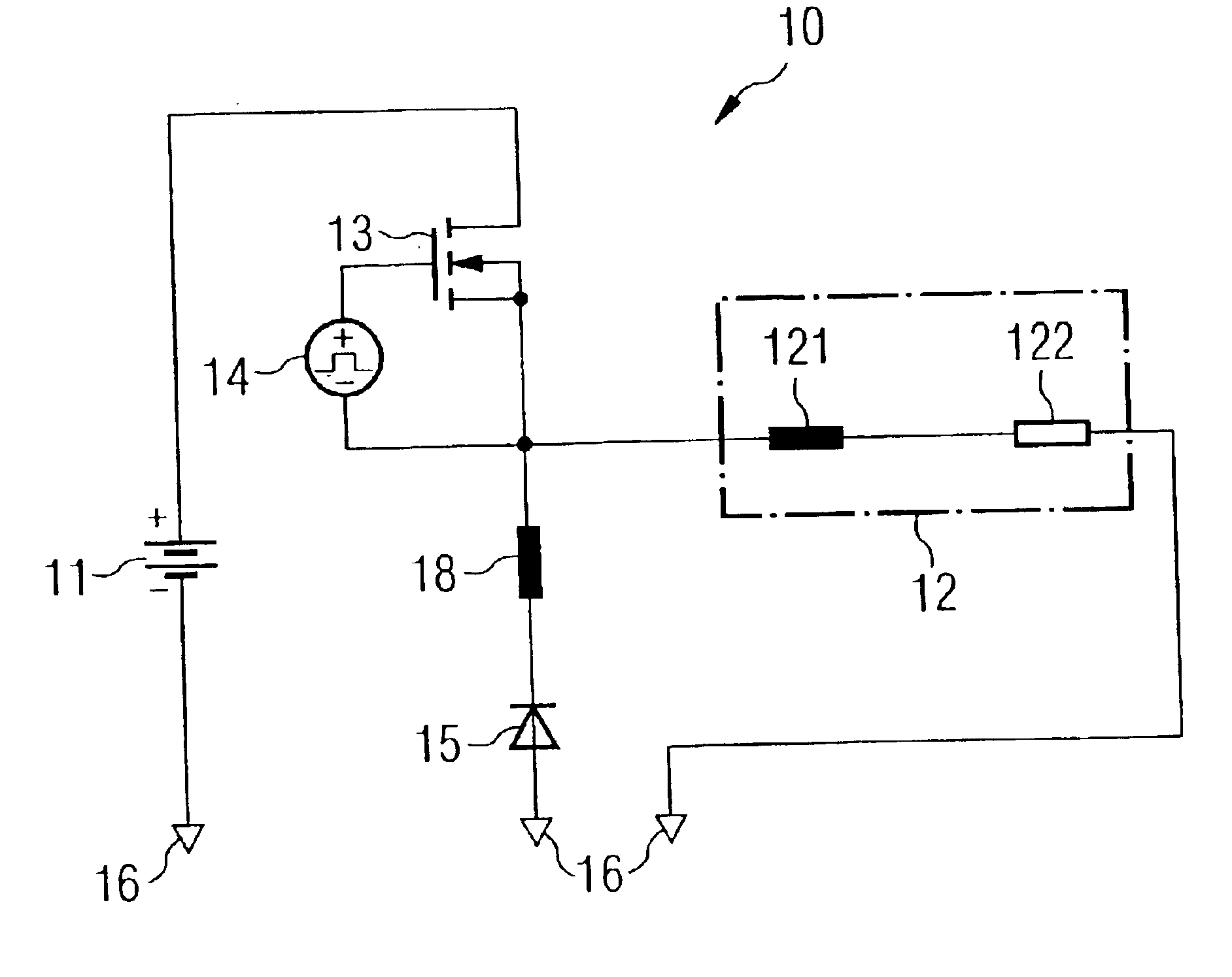
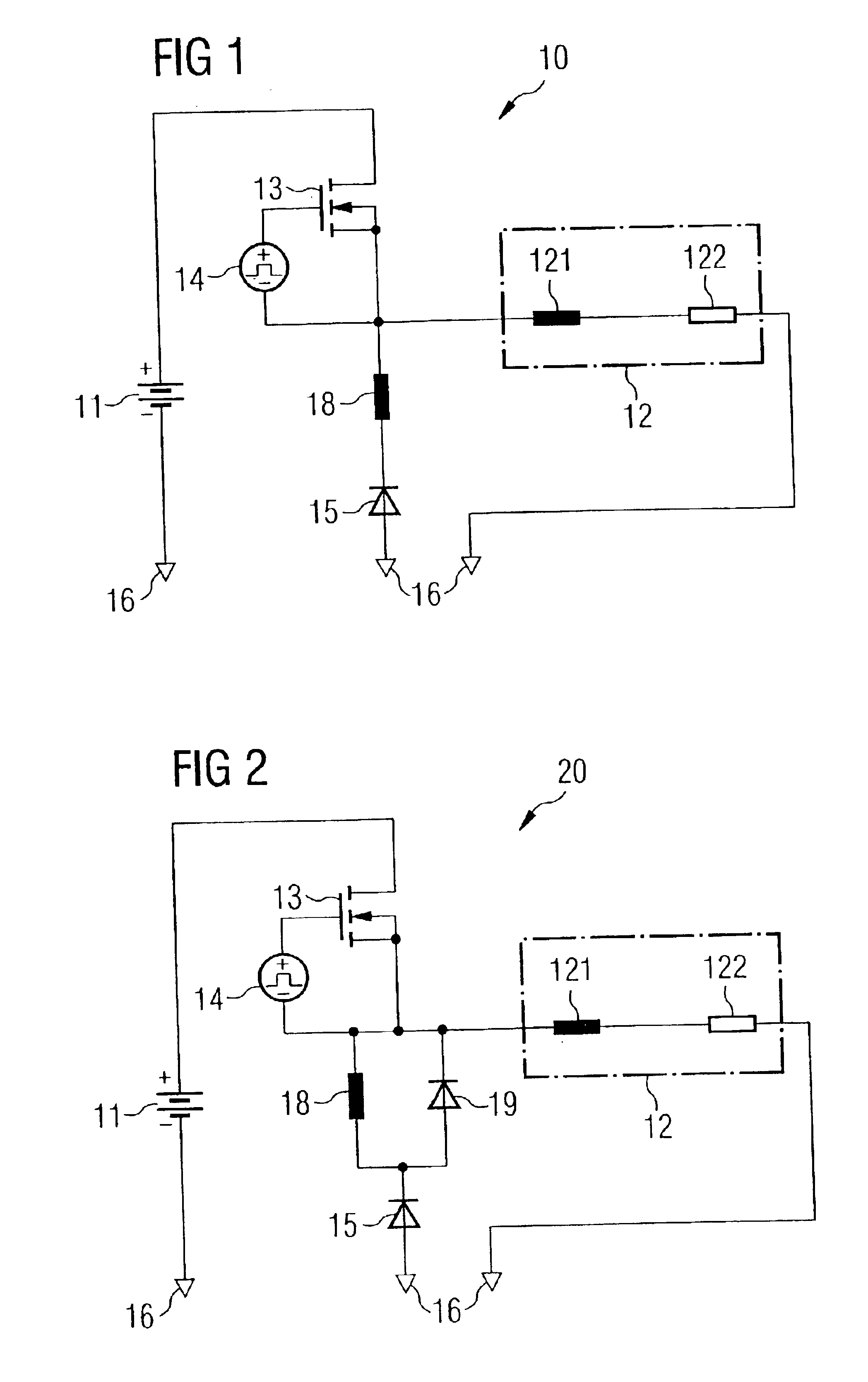
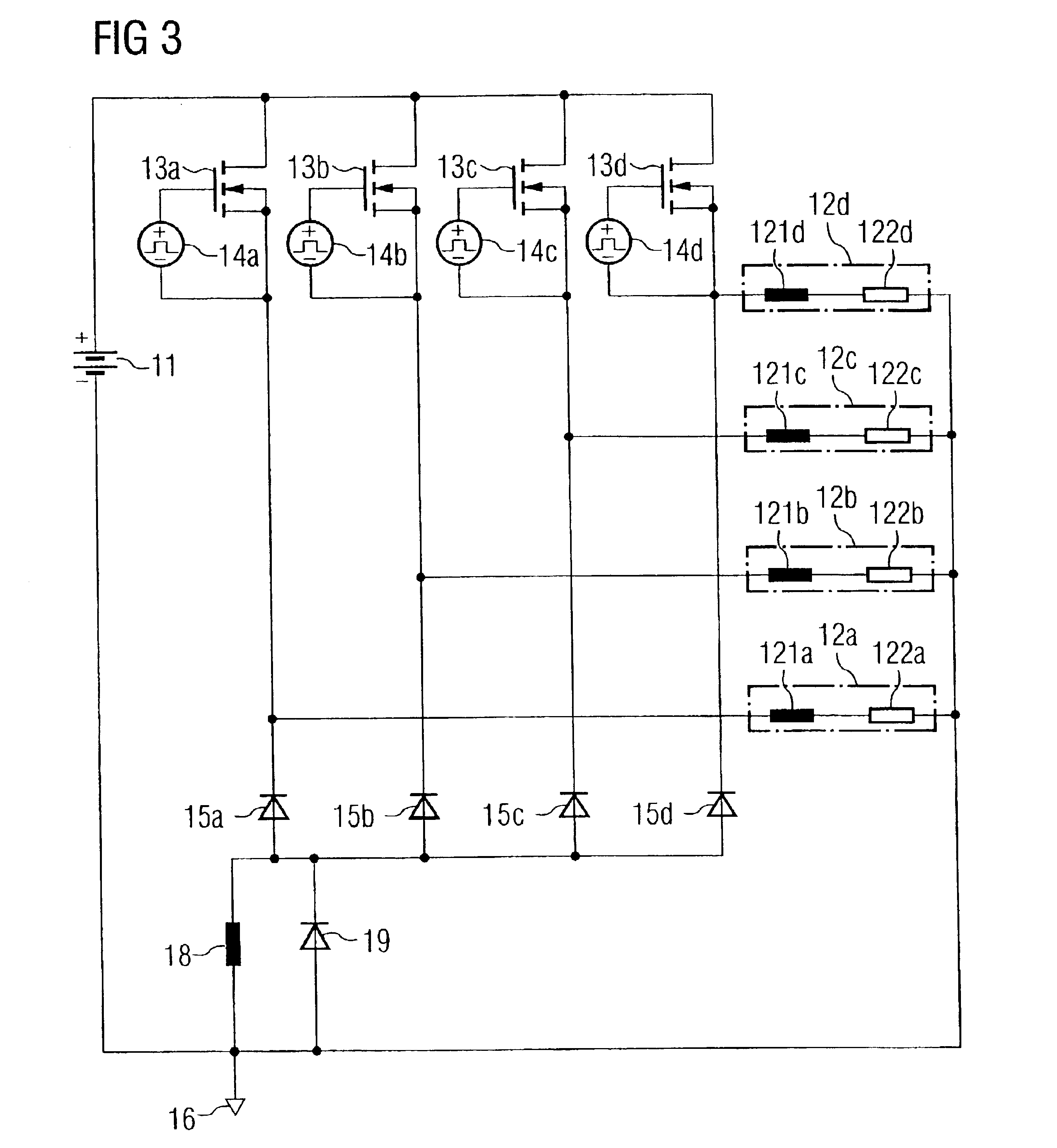
[0034]FIG. 5 represents a prior-art basic circuit 50 for high-speed switching of an inductive load 12. FIG. 7 is a schematic representation of the signals occurring in the circuit. To the inductive load 12, which is shown as a combination of the actual inductance 121 and the ohmic resistance 122 of the coil winding of a magnetic valve, in the turned-on state, an exciter voltage is supposed to be applied by a power supply source 11. To ensure the fastest possible switching operation at a specific inductance 121, a comparatively high exciter voltage is selected. In this present context, this means an exciter voltage which is at least high enough so that the coil resistance 122 is not sufficient to effectively limit the current ISP (FIG. 7c) through the coil 12 to a desired value. It is therefore necessary to otherwise limit the coil current ISP during the activation phase of the magnetic valve. For that purpose, the switching transistor 13, which closes the power circuit comprising th...


PUM

PropertyMeasurementUnit
timeaaaaaaaaaa
timeaaaaaaaaaa
voltageaaaaaaaaaa

Abstract

A circuit arrangement for switching an inductive load (12, 12a-d) with connections to a power supply source (11, 11′, 11″) by means of which an exciter voltage can be applied to the inductive load (12, 12a-d) in a switched-on state is described, comprising switching means by means of which, depending on a control signal, a power circuit comprising the inductive load (12, 12a-d) and the power supply source connections, can be closed when switched from the switched-off to the switched-on state and opened when switched from the switched-on to the switched-off state, furthermore comprising a first diode (15, 15a-d, 15a′-c′, 15a″-c″) arranged in parallel with the inductive load (12, 12a-d) and so as to block in the switched-on state. This present invention is characterized in that an additional commutation inductance (18) is provided which is arranged in parallel with the inductive load (12, 12a-d) and in series with the first diode (15, 15a-d, 15a′-c′, 15a″-c″).

Description

BACKGROUND OF THE INVENTION[0001]This present invention refers to a circuit arrangement for switching an inductive load with connections to a power supply source by means of which an exciter voltage can be applied to the inductive load in a switched-on state, comprising switching means by means of which, depending on a control signal, a power circuit comprising the inductive load and the power supply source connections can be opened when switched from the switched-off state to the switched-on state and can be closed when switched from the switched-on state to the switched-off state as well as furthermore comprising a first diode which is connected in parallel with the inductive load and arranged so as to block in the switched-on state.[0002]Such circuits are frequently used wherever rapid mechanical movements are electrically controlled, e.g. in magnetic valves, in particular magnetic injection valves in combustion engines. In this case, the inductive load is e.g. an electromagnet c...

Claims


Application Information

Patent Timeline
Patent Type & Authority Patents(United States)
IPC IPC(8): H03K17/687H03K17/0814H03K17/16H03K17/08H03K17/693
CPCH03K17/08142H03K17/162H03K17/6871H03K17/693
Inventor BOLZ, STEPHANLUGERT, GUNTERGOSER, GERHARD
Owner SIEMENS AG
Why Eureka
Try Eureka