Pixel array

a technology of pixel array and monolayer, applied in the manufacture of electrode systems, optical radiation measurement, record information storage, etc., to achieve the effect of wide application range, high density memory, and altered transparency or reflectivity of monolayers

Inactive Publication Date: 2005-07-19
THE OHIO STATE UNIV RES FOUND
View PDF10 Cites 30 Cited by
  • Summary
  • Abstract
  • Description
  • Claims
  • Application Information

AI Technical Summary

Benefits of technology

[0015]As used herein, the term “strongly coupled electronically” is used to indicate that the substrate(s) and monolayer share common molecular orbital(s) (one or more), and thus that electrons are delocalized over both the monolayer and substrate. This also refers, in the case of an organic moiety, to electronic coupling that is at a level greater than the aliphatic equivalent of the bond in question. A conjugated bond is one example of strong electronic coupling. At least some of the important features of the present invention are believed to be due to perturbation of the molecule's orbital(s) by the substrate, which stems from strong electronic coupling. The chemical monolayer of the present invention thus allows for the creation of a relatively large number of molecules conducting in parallel, the conduction being essentially parallel to the axis of the molecular units.
[0059]The present invention also includes field emitter devices, analogous to those that are the basis of flat panel displays. In these devices, the chemical monolayers of the present invention serve to enhance the efficiency of electron emission in response to applied potential. Electrons emitting from the monolayer may be allowed to strike a light emitter such as a fluorophore-containing surface. These devices may be used to create flat panel displays and screens.

Problems solved by technology

Naturally, depending on the degree of conductivity of the monolayer and its constituent molecular units, the monolayer junctions and devices may tolerate greater or lesser number and / or size of shorts attendant to non-uniformity in the contact between the monolayer and the electrically contacted substrate or conductive components.

Method used


Image

  • Pixel array
  • Pixel array
  • Pixel array

Examples


Embodiment Construction

)

[0084]In accordance with the foregoing summary, the following presents a detailed description of the preferred embodiment of the invention that is currently considered to be the best mode.

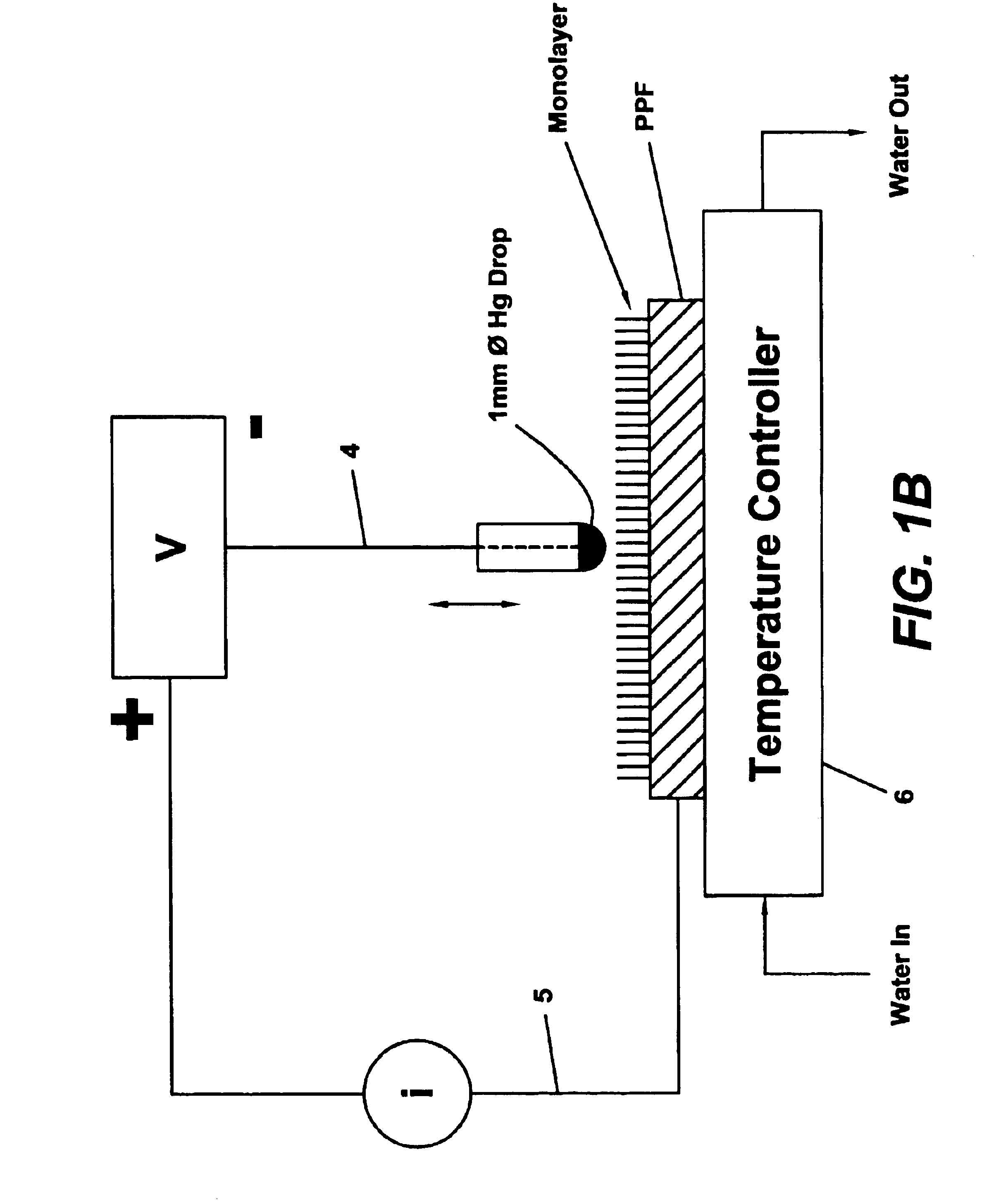
[0085]FIG. 1A shows a schematic of a microelectronic junction in accordance with one embodiment of the present invention. FIG. 1A shows a first conductive member 1 or substrate such as a carbon pyrolyzed photoresist film (“PPF”). To this first conductive member 1 is attached a single layer of a plurality of nitroazobenzene molecules (the “chemical monolayer”), covalently bonded to the carbon PPF. The chemical monolayer 2 is disposed between the first conductive member 1 and the second conductive member 3 (i.e. a liquid such as a mercury drop in a device shown in FIG. 1B), with a layer thickness as small as about 1.5 nm. Covalent bonding between the PPF film and the carbon leads to strong, electronic coupling between the molecular monolayer and the carbon PPF. In a finished device, the second condu...


PUM

PropertyMeasurementUnit
roughnessaaaaaaaaaa
roughnessaaaaaaaaaa
mean roughnessaaaaaaaaaa

Abstract

The present invention includes a chemical monolayer construction that comprises: (a) a substrate having a contact surface; and (b) a plurality of substantially parallel molecular units, wherein said molecular units are attached to said substrate so as to be strongly coupled electronically to said substrate, such as through a conjugated bond. The present invention also includes electronic circuit components and devices including a chemical monolayer construction of the present invention.

Description

RELATED APPLICATIONS[0001]This application is a divisional application of U.S. application Ser. No. 09 / 755,437 filed Jan. 5, 2001, the contents of which is incorporated herein by reference.TECHNICAL FIELD OF THE INVENTION[0002]The present invention is in the field of chemical monolayers and microelectronic junctions, and includes chemical sensors, photosensors and other devices containing them.BACKGROUND OF THE INVENTION[0003]The term “molecular electronics” has been used to describe phenomena or devices that include a molecule as a circuit element (1,2). The motivation for the field is the prospect of making extremely small (potentially one molecule) electronic components with a much wider range of functions than conventional semiconductor electronic devices. If molecular devices become practical, a wide variety of applications in microelectronics, computing, imaging and display technology and chemical sensing can be envisioned. The large majority of proposed molecular electronic d...

Claims


Application Information

Patent Timeline
Patent Type & Authority Patents(United States)
IPC IPC(8): G11B9/00G01N27/12B82B1/00C30B29/00G01J1/02G11B5/127G11B5/33H01J9/02H01J29/04H01J31/12H01L29/06H01L29/12H01L29/66H01L51/05H01L51/42
CPCB82Y10/00G11B9/14G11B9/1472G11C11/14H01L51/0595G11B9/149B05D1/185Y10T428/268Y10T428/261Y10T428/31536Y10T428/31504G11B9/04H10K10/701
Inventor MCCREERY, RICHARD L.
Owner THE OHIO STATE UNIV RES FOUND
Why Eureka
Try Eureka