Method for producing a contactless chip card using transfer paper
a technology of transfer paper and chip card, which is applied in the direction of dielectric characteristics, printed circuit non-printed electric components association, instruments, etc., can solve the problems of high cost of copper and etching process, high cost of antenna on pvc support, and high cost of sophisticated machineries. , to achieve the effect of low cost pri
- Summary
- Abstract
- Description
- Claims
- Application Information
AI Technical Summary
Benefits of technology
Problems solved by technology
Method used
Image

Examples
first embodiment
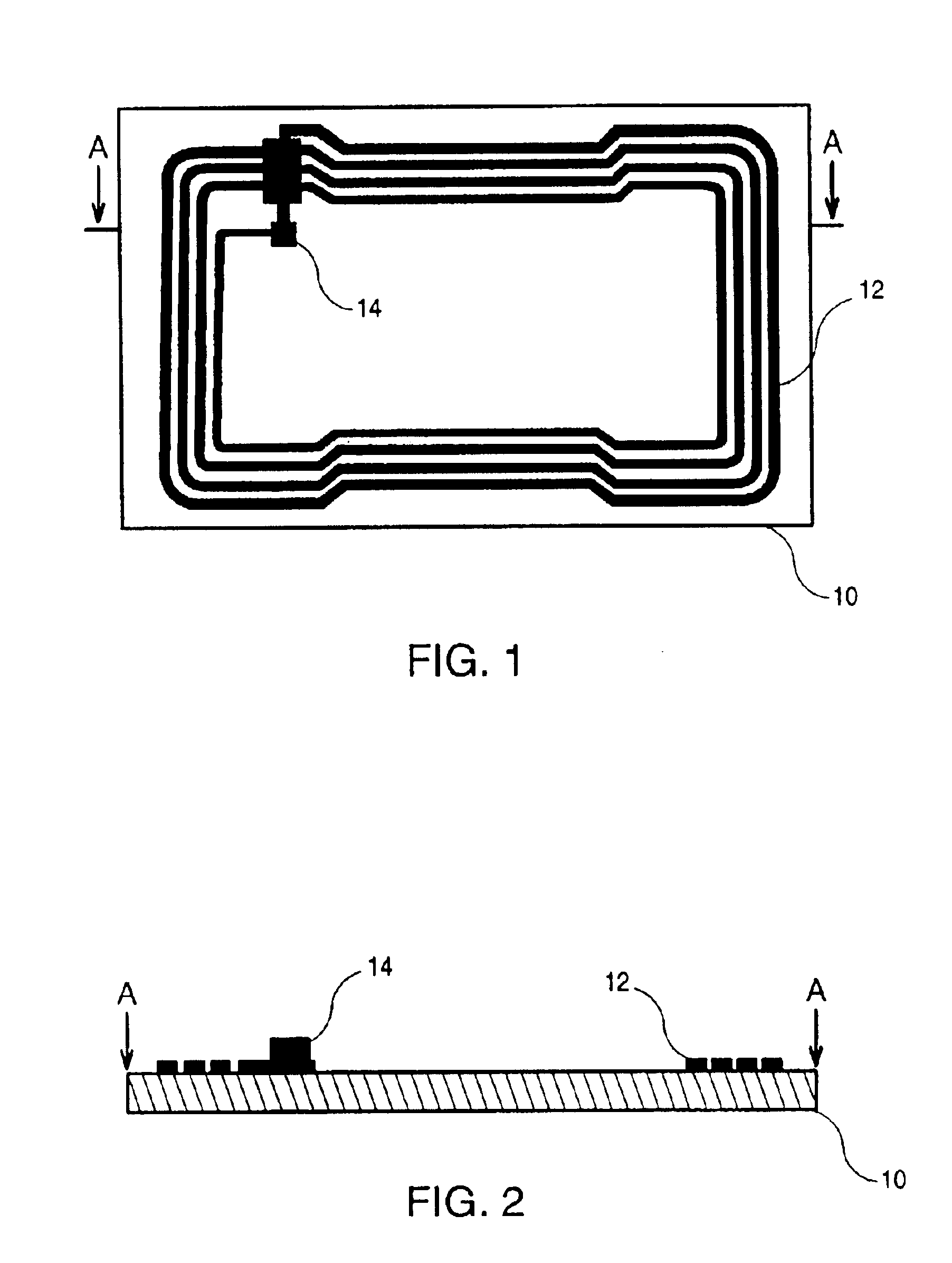
[0030]Once the antenna has been produced, the chip is connected to the antenna while it is still on the transfer paper sheet. The transfer paper sheet 10 bearing the screen-printed antenna 12 and the chip 14 (which are already connected) are shown in FIG. 1. Different methods may be used to connect the chip 14 to the antenna 12. A first embodiment includes the following steps:[0031]positioning the chip on the transfer paper so that the chip's contacts are located opposite the antenna's contacts, and[0032]exerting pressure on the chip so that its contacts deform the transfer paper and the antenna's contacts. The transfer paper sheet and the antenna's contacts remain deformed after the pressure is released, thus providing an extensive area of contact between the contacts on the chip and those on the antenna.
second embodiment
[0033] connecting the chip includes the following steps:[0034]coating the antenna's contacts with a conductive adhesive, and[0035]positioning the chip on the transfer paper so that the contacts of said chip become submerged in said conductive adhesive opposite the antenna's contacts.
[0036]FIG. 2 shows a longitudinal section through axis A—A of the transfer paper sheet. The transfer paper sheet 10 bears the antenna 12 in the form of screen-printed turns. The chip 14 is connected to the antenna 12.
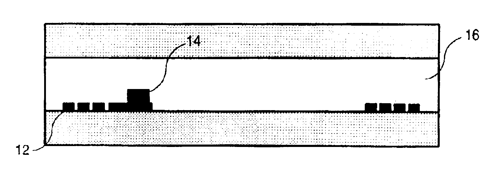
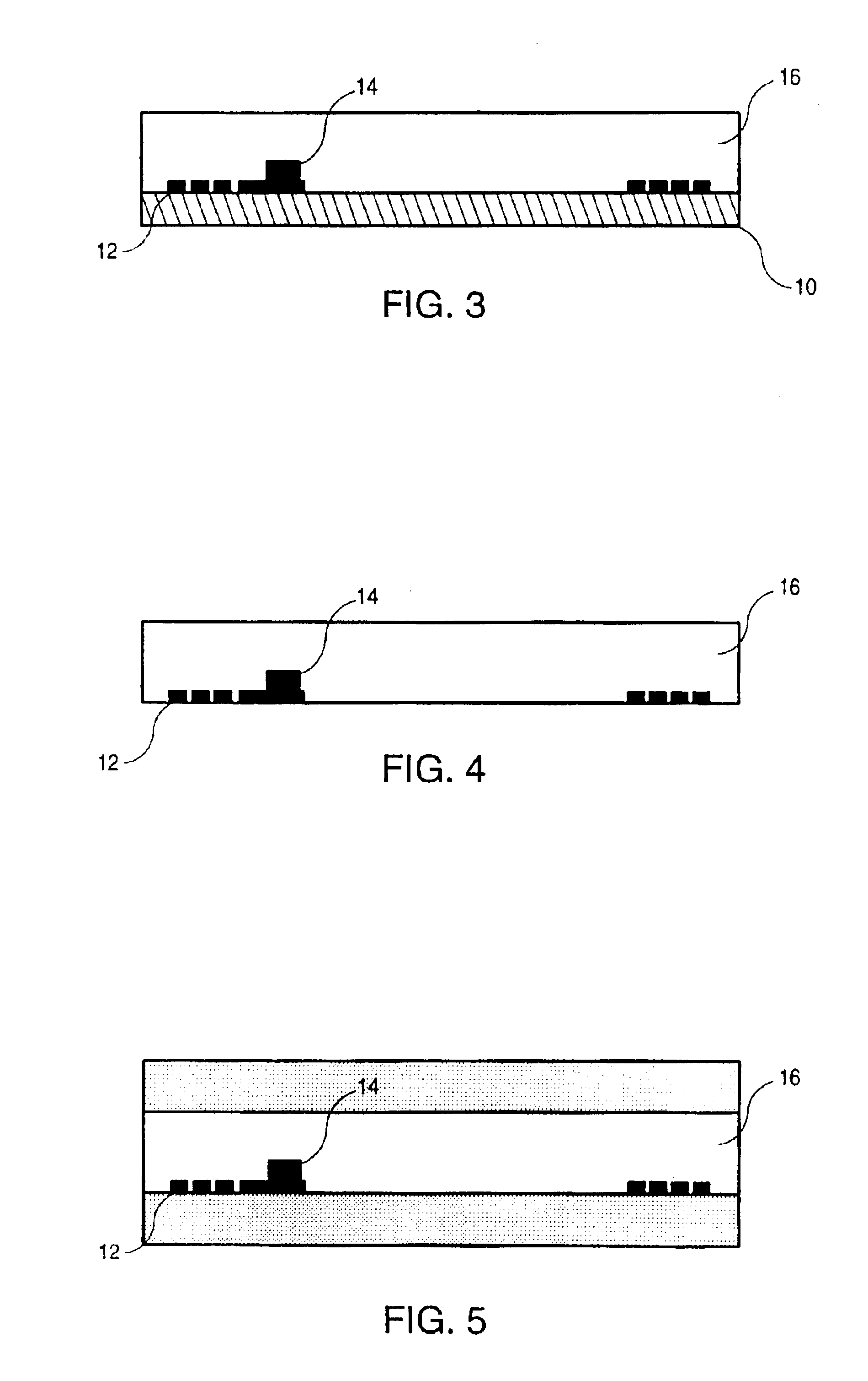
[0037]When the chip has been connected to the antenna, the transfer paper sheet is laminated with a sheet of plastic material which constitutes the antenna support. This lamination step is accomplished by hot press molding. FIG. 3 shows the transfer paper sheet 10 and the plastic antenna support 16. According to a preferred embodiment, the plastic material might be either PVC or PET. From FIG. 3, it can be seen that, once the lamination step has been performed, the screen-printed antenna 12 ...
PUM
| Property | Measurement | Unit |
|---|---|---|
| Vicat point | aaaaa | aaaaa |
| Vicat point | aaaaa | aaaaa |
| temperature | aaaaa | aaaaa |
Abstract
Description
Claims
Application Information
 - R&D
- Intellectual Property
- Life Sciences
- Materials
- Tech Scout
- Unparalleled Data Quality
- Higher Quality Content
- 60% Fewer Hallucinations
Browse by: Latest US Patents, China's latest patents, Technical Efficacy Thesaurus, Application Domain, Technology Topic, Popular Technical Reports.
© 2025 PatSnap. All rights reserved.Legal|Privacy policy|Modern Slavery Act Transparency Statement|Sitemap|About US| Contact US: help@patsnap.com