
Semiconductor device having a high breakdown voltage for use in communication systems

a technology of high breakdown voltage and semiconductor device, which is applied in the direction of semiconductor device/discharge tube, low-noise amplifier, solid-state device, etc., can solve the problems of breakdown voltage, power consumption increase, and difficulty in implementing transistors

Inactive Publication Date: 2005-06-07
PANASONIC CORP
View PDF15 Cites 26 Cited by
  • Summary
  • Abstract
  • Description
  • Claims
  • Application Information

AI Technical Summary

Benefits of technology

[0014]It is therefore an object of the present invention to provide a semiconductor device which simultaneously achieves a high breakdown voltage and a low resistance as described above, particularly a semiconductor device excellent in RF characteristic and equipment for a communication system using the semiconductor device.

Problems solved by technology

However, the conventional semiconductor device and the equipment for a communication system using the conventional semiconductor device have the following problems.
As a result, power consumption is increased.
Due to such a trade-off, it has been difficult to implement a transistor which is high in breakdown voltage and low in resistance.
Such a problem is also encountered if the transistor is a bipolar transistor.
However, the power is low because of the trade-off between a high breakdown voltage and a low resistance that has not been overcome so that a large number of elements are required and it is difficult to scale down the device.
To maintain the base station, therefore, a cooling device having a high cooling ability and high running cost are necessary.
As the frequency of the RF signal is higher, however, reflected waves from the MESFETs exert multiple effects so that it is difficult to achieve impedance matching.
This causes the disadvantage of increased labor required by trimming for impedance adjustment.

Method used


Image

  • Semiconductor device having a high breakdown voltage for use in communication systems
  • Semiconductor device having a high breakdown voltage for use in communication systems
  • Semiconductor device having a high breakdown voltage for use in communication systems

Examples


example 1

of Specific Structure of HEMT

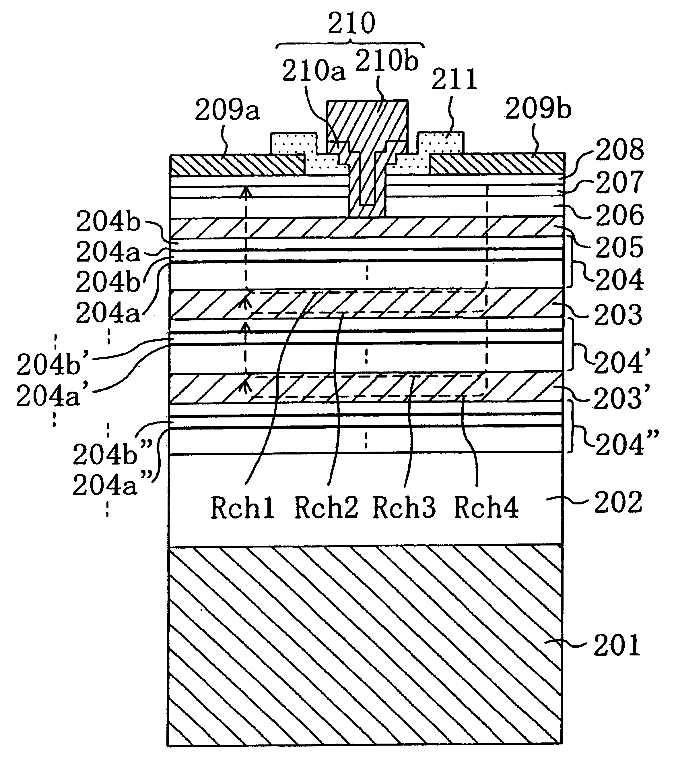
[0168]FIG. 17 is a schematic cross-sectional view showing a specific structure of the HEMT in a first example of the embodiment of the present invention. As shown in the drawing, an undoped InAlAs layer 202 (in which ratios of components are In0.52Al0.48As) with a thickness of about 200 nm, an undoped InGaAs layer 203 (in which ratios of components are In0.53Ga0.47As) with a thickness of about 15 nm, a multiple δ-doped InAlAs layer 204 (in which ratios of components are In0.52Al0.48As) composed of five n-type doped layers 204a (containing Si as an impurity) each having a thickness of about 1 nm and six undoped layers 204b each having a thickness of about 10 nm which are alternately stacked (of which the uppermost and lowermost layers are undoped) to serve as a carrier supplying layer with a thickness of about 65 nm, an InP layer 205 serving as an etching stopping layer with a thickness of about 5 nm, an n-InAlAs layer 206 (in which ratios of components a...

example 2

of Specific Structure of HEMT

[0178]FIG. 19 is a schematic cross-sectional view showing a specific structure of the HEMT in a second example of the embodiment of the present invention. In the present example, as shown in the drawing, an undoped InAlAs layer 202 (in which ratios of components are In0.52Al0.48As) with a thickness of about 200 nm, a multiple δ-doped InAlAs layer 204″ (in which ratios of components are In0.52Al0.48As) composed of five n-type doped layers 204a (containing Si as an impurity) each having a thickness of about 1 nm and six undoped layers 204b each having a thickness of about 10 nm which are alternately stacked (of which the uppermost and lowermost layers are undoped) to serve as a carrier supplying layer with a thickness of about 65 nm, an undoped InGaAs layer 203′ (in which ratios of components are In0.53Ga0.47As) with a thickness of about 15 nm, a multiple δ-doped InAlAs layer 204′ (in which ratios of components are In0.52Al0.48As) composed of five n-type d...


PUM


Abstract

A HEMT has an InAlAs layer (202), an InGaAs layer (203), a multiple δ-doped InAlAs layer (204) composed of n-type doped layers (204a) and undoped layers (204b) which are alternately stacked, an InP layer (205), a Schottky gate electrode (210), a source electrode (209a), and a drain electrode (209b) on an InP substrate (201). When a current flows in a region (channel region) of the InGaAs layer (203) adjacent the interface between the InGaAs layer (203) and the multiple δ-doped InAlAs layer (204), a breakdown voltage in the OFF state can be increased, while resistance to the movement of carriers passing through the multiple δ-doped InAlAs layer (204) as a carrier supplying layer is reduced.

Description

TECHNICAL FIELD[0001]The present invention relates to a semiconductor device functioning as a semiconductor power device having a high breakdown voltage to be used to handle an RF signal and to equipment for a communication system using the semiconductor device.BACKGROUND ART[0002]In recent years, new semiconductor materials (including so-called semi-insulating materials) for implementing semiconductor devices which have special functions and are particularly excellent in specific characteristics such as an RF characteristic, a light-emitting characteristic, and a breakdown voltage characteristic have been under vigorous development. Of the semiconductor materials, e.g., a semiconductor containing an indium phosphide (InP) as a main component thereof is expected to be applied to a next-generation RF device, high-temperature operating device, and the like because the electron mobility and the saturation velocity of electrons are higher than those of silicon (Si) which is a typical se...

Claims


Application Information

Patent Timeline
IPC IPC(8): H01L29/778H01L21/70H01L29/66H01L21/8252H01L27/06H03F3/60H01L29/20H01L29/02
CPCH01L21/8252H01L27/0605H01L29/7785H03F3/601H03F2200/294H01L29/2003
Inventor YOKOGAWA, TOSHIYASUZUKI, ASAMIRADEGUCHI, MASAHIROYOSHII, SHIGEOFURUYA, HIROYUKI
Owner PANASONIC CORP
Learn More