Method of forming ohmic electrode

Inactive Publication Date: 2005-05-03
SHARP FUKUYAMA LASER CO LTD
View PDF5 Cites 11 Cited by
  • Summary
  • Abstract
  • Description
  • Claims
  • Application Information

AI Technical Summary

Benefits of technology

[0007]In view of the above circumstances the present invention contemplates a method of forming an ohmic electrode having low resistance, hardly peeling off an n type nitride-based compound semiconductor layer, and providing good ohmic contact.

Problems solved by technology

The above reported Hf / Al electrode, however, is formed by stacking Hf and Al layers without particularly controlling the concentrations of Hf and Al contained in the electrode.
Furthermore, the electrode can peel off the semiconductor layer and thus fail to provide good ohmic contact.

Method used


Image

  • Method of forming ohmic electrode
  • Method of forming ohmic electrode
  • Method of forming ohmic electrode

Examples


examples

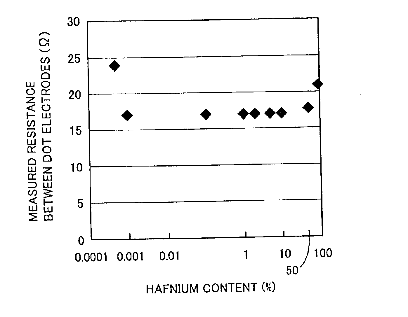
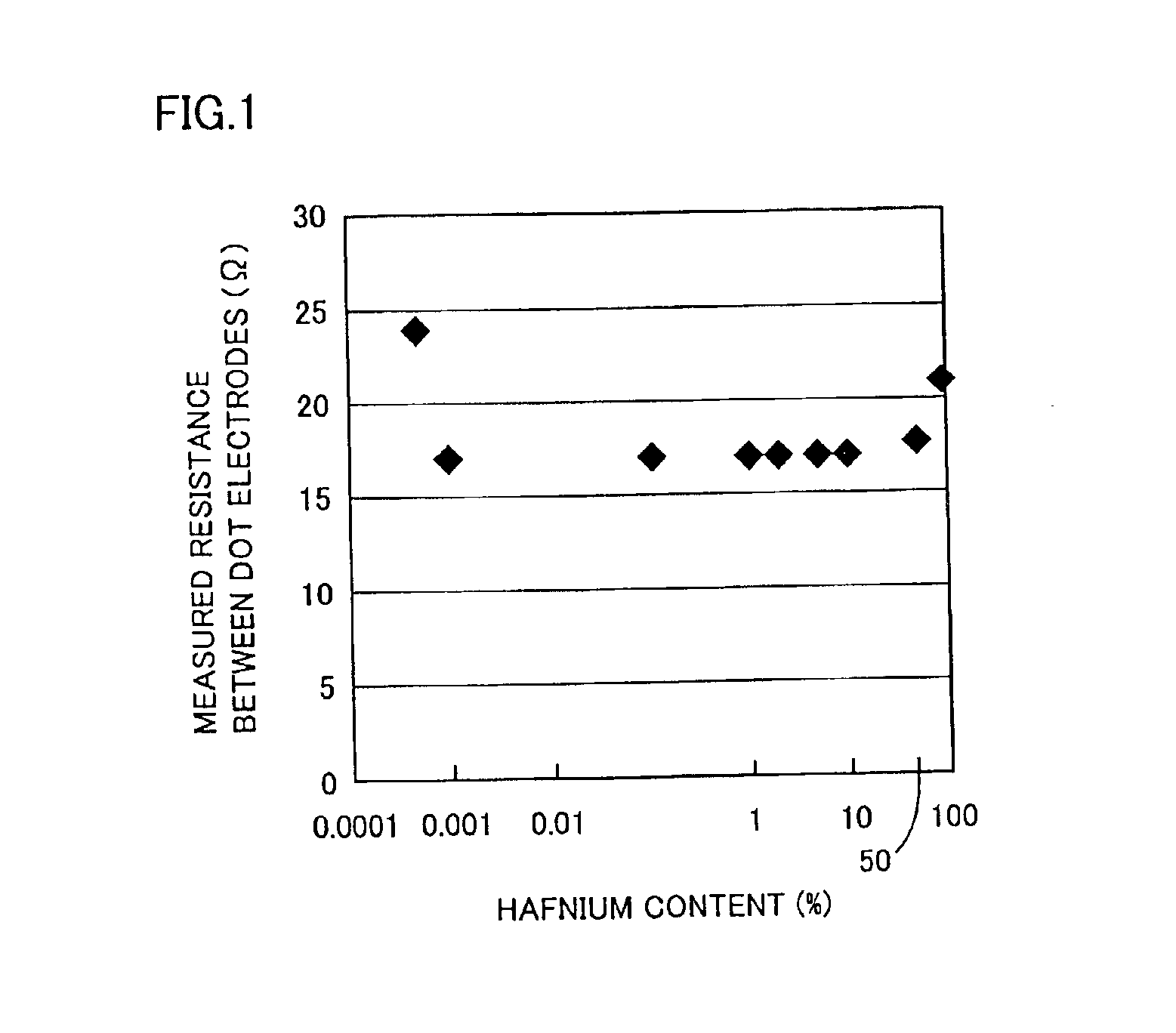
[0044]Hereinafter examples are used to more specifically describe a light emitting nitride-based compound semiconductor device using an ohmic electrode of the present invention.

first example

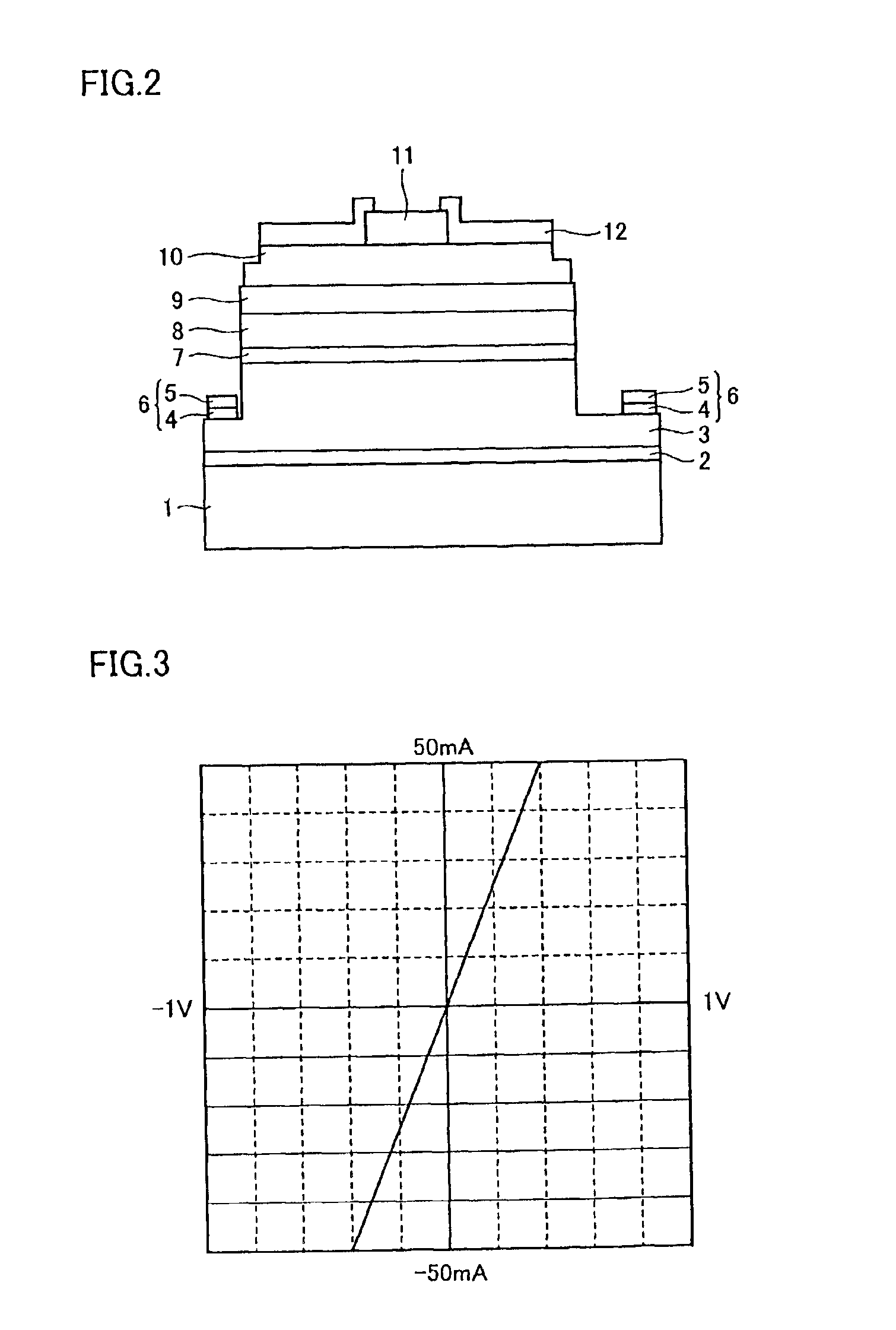
[0045]With reference to FIG. 2, a first example provides a light emitting nitride-based compound semiconductor device including a sapphire substrate 1, a buffer layer 2, an n type nitride-based compound semiconductor layer 3, an ohmic electrode 4, a pad electrode 5, an n type electrode 6, a light emitting layer 7, a p type clad layer 8, a p type contact layer 9, a p type ohmic electrode 10, a p type pad electrode 11, and a transparent conductive film 12.

[0046]The light emitting nitride-based compound semiconductor device of the first example is fabricated, as specifically described hereinafter.

[0047]On sapphire substrate 1 buffer layer 2 is formed and thereon n type nitride-based compound semiconductor layer 3 is formed of silicon (Si) doped GaN. Then on semiconductor layer 3 multiple quantum well light emitting layer 7 is formed of a barrier layer formed of GaN and a well layer formed of InGaN. On light emitting layer 7 p type clad layer 8 is formed of Mg doped AlGaN. On clad layer...

second example

[0064]In the first example, Hf and Al layers are provided by vapor deposition and then annealed in a vacuum to form an ohmic electrode with the Hf and Al layers mixed together. In a second example, in depositing a Hf layer or an Al layer a wafer is heated to form an ohmic electrode having a layer with Hf and Al mixed together.

[0065]With reference to FIG. 5, the second example provides a light emitting nitride-based compound semiconductor device including a sapphire substrate 21, a buffer layer 22, an n type nitride-based compound semiconductor layer 23, an ohmic electrode 24, a pad electrode 25, an n type electrode 26, a light emitting layer 27, a p type clad layer 28, a p type contact layer 29, a p type ohmic electrode 110, a p type pad electrode 111, and a transparent conductive film 112

[0066]The light emitting nitride-based compound semiconductor device of the second example is fabricated, as specifically described hereinafter.

[0067]The same process as described in the first exam...


PUM


Abstract

There is provided a method of forming an ohmic electrode, including the steps of: forming a hafnium layer on a surface of an n type nitride-based compound semiconductor layer to have a thickness of 1 to 15 nm; forming an aluminum layer on the hafnium layer; and annealing the hafnium layer and the aluminum layer to form a layer formed of hafnium and aluminum mixed together.

Description

BACKGROUND OF THE INVENTION[0001]1. Field of the Invention[0002]The present invention relates generally to methods of forming an ohmic electrode formed on an n type nitride-based compound semiconductor layer, and particularly to methods of forming an ohmic electrode having low resistance, hardly peeling off, and providing good ohmic contact.[0003]2. Description of the Background Art[0004]It has conventionally been known that a nitride-based compound semiconductor represented for example by InxGayAl1-x-yN can be used as a blue light emitting device, wherein 0≦x≦1, 0≦y≦1 and x+y≦1, and in recent years blue light emitting diodes, violet semiconductor lasers and the like are being studied. These light emitting diodes and semiconductor lasers need to externally receive a current. Accordingly, the material(s) of an ohmic electrode provided thereto and the technique used to form the same are significantly important.[0005]A typical ohmic electrode formed on an n type nitride-based compound ...

Claims


Application Information

Patent Timeline
IPC IPC(8): H01L29/45H01L29/40H01L33/00H01L21/02H01L21/285H01L29/20H01L29/02H01L21/28H01L33/32H01L33/42H01L33/62H01S5/042H01S5/323H01S5/343
CPCH01L33/40H01L29/452H01L21/28575H01L29/2003H01L33/32
Inventor FUDETA, MAYUKOHATA, TOSHIO
Owner SHARP FUKUYAMA LASER CO LTD
Why Eureka
Try Eureka