Test circuit and multi-chip package type semiconductor device having the test circuit

a test circuit and semiconductor technology, applied in the direction of semiconductor/solid-state device details, resistance/reactance/impedence, instruments, etc., can solve the problems of device having a damaged chip, function test may not be able to find a damaged chip, and the peripheral circuit formed near the pads may be damaged, so as to test the mcp semiconductor device accurately and quickly

Inactive Publication Date: 2005-04-26
LAPIS SEMICON CO LTD
View PDF7 Cites 0 Cited by
  • Summary
  • Abstract
  • Description
  • Claims
  • Application Information

AI Technical Summary

Benefits of technology

[0015]It is therefore an object of the invention to resolve the above-described problem in an MCP semiconductor device and provide an MCP semiconductor device having a test circuit for testing the MCP semiconductor device accurately and rapidly.

Problems solved by technology

As a result, a peripheral circuit, which is formed near the pads, may be damaged by the surges.
However, when the damage is not so critical to a peripheral circuit, an MCP semiconductor device having a damaged chip may not be found by the function test because the damaged circuit operates normally.
Since it is difficult to find an MCP semiconductor device having a damaged chip by a function test, an MCP semiconductor device having a damaged chip is found by measuring a leakage current.
However, as described above, the function test may not be able to find a damaged chip when the damage is not critical.
In the worst case, the MCP semiconductor device having the damaged chip malfunctions, and it causes the system to malfunction.
However, there are some problems with this measurement.
As a result, a long time is required for measuring the consuming current (IDDS) under the conduction that an operation of all chips is halted.
That is, when MCP semiconductor device includes a chip such as a memory chip or similar kinds, it may be impossible to set the value of the electric current to be caused to flow in the chip to zero (“0”), depending on the voltage level that is applied to each terminal.
As a result, it is difficult to obtain accurate measurement results.
Moreover, if one of the two chips is an analog circuit such as an A / D converter, it is difficult to fix the internal pad P101, P102 to the predetermined voltage level.
As described above, it is not easy to test the internal terminal pads and their peripheral circuits formed on each chip, according to the structure of the MCP semiconductor device

Method used


Image

  • Test circuit and multi-chip package type semiconductor device having the test circuit
  • Test circuit and multi-chip package type semiconductor device having the test circuit
  • Test circuit and multi-chip package type semiconductor device having the test circuit

Examples


first preferred embodiment

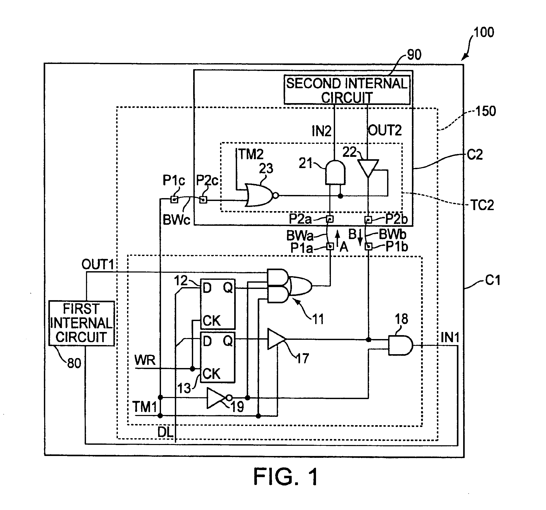
[0028]Referring to FIG. 1, a multi-chip package type semiconductor device (hereinafter “an MCP semiconductor device”) 100 includes a first semiconductor chip (hereinafter “a first chip”) C1 and a second semiconductor chip (hereinafter “a second chip”) C2 mounted on the first chip C1.

[0029]The first chip C1 includes a first test circuit TC1 and internal terminal pads (hereinafter “internal pads”) P1a, P1b, P1c. The second chip C2 includes a second test circuit TC2 and internal pads P2a, P2b, P2c. The internal pad P1a is connected to the internal pad P2a by a bonding wire BWa. The internal pad P1b is connected to the internal pad P2b by a bonding wire BWb. The internal pad P1c is connected to the internal pad P2c by a bonding wire BWc. In the normal operation of the MCP semiconductor device, a signal from the first chip C1 is transferred to the second chip C2 through the bonding wire BWa in the direction of an arrow A shown in FIG. 1. A signal from the second chip C2 is transferred to...

second preferred embodiment

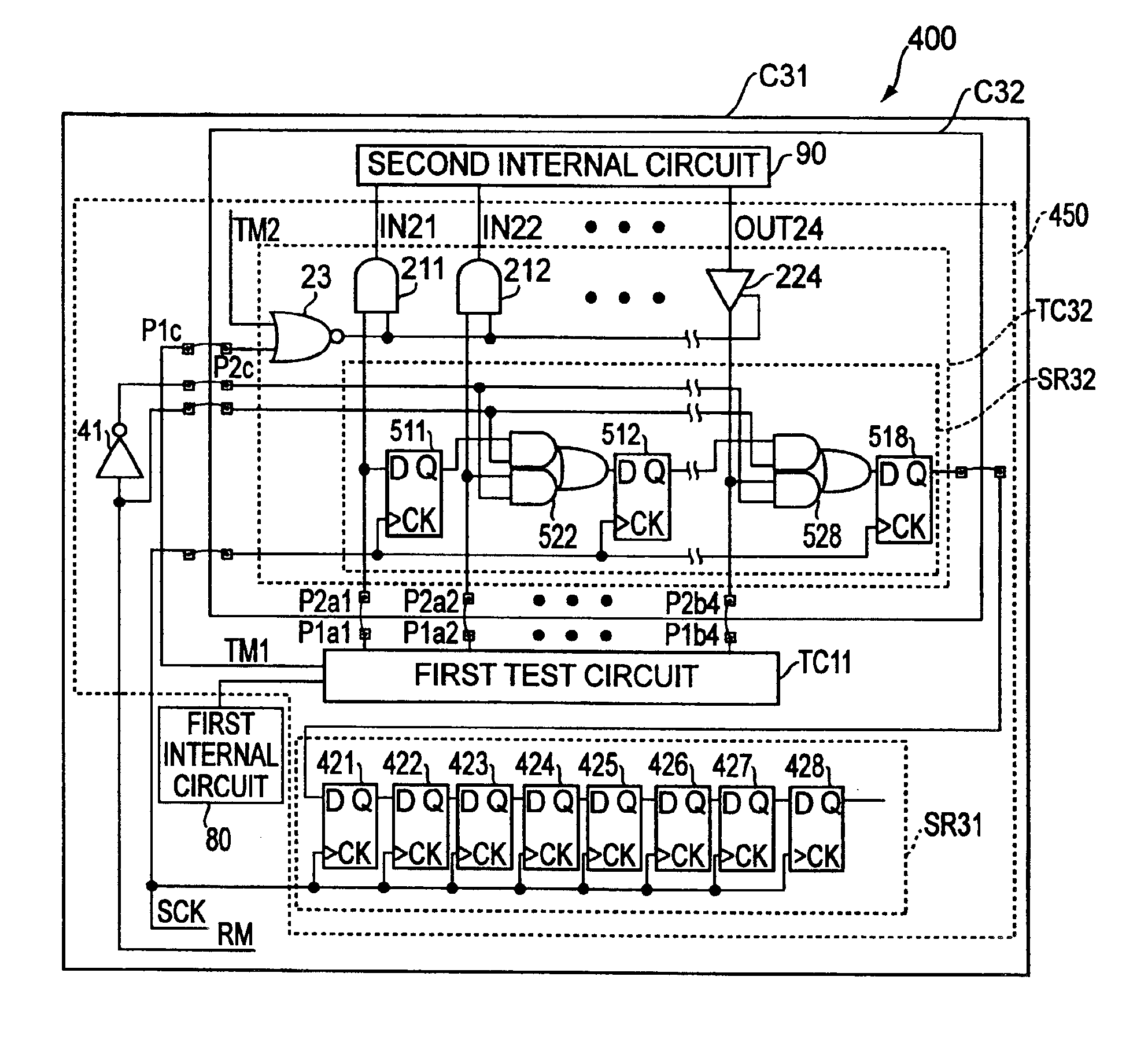
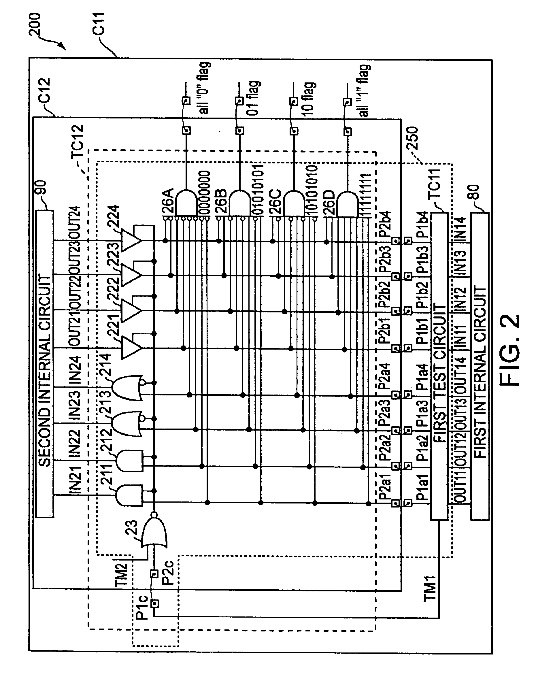
[0053]In the first embodiment, the first and second test circuit TC1, TC2 are capable of the first and second chips C1, C2, each of which has two pairs of the internal pads (P1a & P1b and P2a & P2b) that transfer some signals. On the other hand, a test circuit 250 of the second embodiment is capable of a first and second chips, each of which has more than two pairs of the internal pads.

[0054]Referring to FIG. 2, an MCP semiconductor device 200 includes a first chip C11 and a second chip C12 mounted on the first chip C11. The first chip C11 includes internal pads P1a1, P1a2, P1a3, P1a4, P1b1, P1b2, P1b3, P1b4, P1c, and the second chip C12 includes internal pads P2a1, P2a2, P2a3, P2a4, P2b1, P2b2, P2b3, P2b4, P2c. Each of the internal pads P1a1 through P1a4 are connected to one of the internal pads P2a1 through P2a4 by a bonding wire, and each of the internal pads P1b1 through P1b4 are connected to one of the internal pads P2b1 through P2b4 by a bonding wire. Further, the internal pad...

third preferred embodiment

[0082]Comparing to the MCP semiconductor device 100 having the test circuit 150 of the first embodiment, an MCP semiconductor device 300 includes a first chip C21 instead of the first chip C1 disclosed in the first embodiment, and the second chip C2. The first chip C21 includes a first test circuit TC21, and the second chip C2 includes the second test circuit TC2. The test circuit 350 is a combination of the first test circuit TC21 and the second test circuit TC2

[0083]Referring to FIG. 3, the first test circuit TC21 includes first and second analog switches SW1, SW2, an external terminal control circuit 32, a first 3-state buffer 37 having one input terminal, one output terminal and one control terminal, a first AND gate 38 having two inputs and one output, and an inverter 39.

[0084]The external terminal control circuit 32 includes second through fifth AND gates 321, 322, 323, 324, each having two inputs and one output, and second and third 3-state buffers 325, 356, each having one i...


PUM


Abstract

A MCP semiconductor device includes at least first and second chips, each of which has internal pads and an internal circuit, encapsulated by a sealing material together. The device further includes a test circuit. The test circuit connects each of the internal pads to one of the internal circuits under a normal operation mode of the device, and disconnect between them under a test mode.

Description

CROSS-REFERENCE TO RELATED APPLICATION[0001]This application claims the priority benefit of Japanese Patent Application No. 2000-320643, filed Oct. 20, 2000, the entire disclosure of which is incorporated herein by reference. This application is a division of applicant's application Ser. No. 09 / 978,630, Oct. 18, 2001 now U.S. Pat. No. 6,762,486.BACKGROUND OF THE INVENTION[0002]1. Field of the Invention[0003]This invention relates to a test circuit capable of a multi-chip package type semiconductor device (MCP semiconductor device) and an MCP semiconductor device having the test circuit.[0004]2. Description of the Related Art[0005]In the related art, there are several types of multi-chip packages in which more than one IC chip can be packaged. One typical multi-chip package is a stack-type multi-chip package that packages at least two IC chips in a stacked manner as shown in FIG. 7. Another typical multi-chip package is a parallel-type multi-chip package that packages at least two IC...

Claims


Application Information

Patent Timeline
Patent Type & Authority Patents(United States)
IPC IPC(8): G01R31/28G01R31/3185G06F11/22H01L21/822H01L27/04
CPCG01R31/318505H01L2224/48091H01L2224/48137H01L2224/49175H01L2924/00014H01L2224/05554H01L2924/3011H01L2924/00
Inventor INOUE, KAZUTOSHIOHIE, MITSUYA
Owner LAPIS SEMICON CO LTD
Why Eureka
Try Eureka