
Area array connector having stacked contacts for improved current carrying capacity

Inactive Publication Date: 2005-04-12
AIRBORN
View PDF28 Cites 58 Cited by
  • Summary
  • Abstract
  • Description
  • Claims
  • Application Information

AI Technical Summary

Benefits of technology

The area array connector of the present invention provides several advantages over conventional interposer designs. First, the area array connector of the present invention provides for an interposer style interconnection system between circuit cards that is capable of carrying both low current signal interconnectors as well as much higher current power interconnectors in a single integrated interposer housing. In addition, the same form of electrical contact can be used for both signal interconnectors and power interconnectors within the area array connector, as a single electrical contact can be used as a signal interconnector, and a number of stacked electrical contacts can be used to form a power interconnector. The integration of signal interconnectors and power interconnectors into a single interposer design provides for lower system cost compared to conventional interposer designs, which generally use separate large, bulky power contacts that are physically separated from the interposer in order to provide power interconnection between circuit cards.
Another advantage of the area array connector of the present invention is that power interconnectors having any required current carrying capacity can be obtained simply by stacking the appropriate number of electrical contacts side-by-side in an appropriately sized aperture in the area array connector. The fact that each individual electrical contact is thin and flat allows for many electrical contacts to be stacked side-by-side in a small area. In contrast, conventional power contacts require the production of a differently sized contact for each incremental increase in required current, leading to expensive retooling costs for the production of the new power contact size.
An additional advantage of using multiple electrical contacts to form a power interconnector in accordance with the principles of the present invention is that the each electrical contact makes a separate and independent connection with the power contact pad on the circuit card. As a result, the reliability of the power interconnector is increased due to the presence of redundant connections. In addition, the total contact resistance of the power interconnector is decreased due to the presence of multiple parallel electrical paths between the contact tips of the electrical connectors and the power contact pads on the circuit card, resulting in improved electrical performance.

Problems solved by technology

In contrast, conventional power contacts require the production of a differently sized contact for each incremental increase in required current, leading to expensive retooling costs for the production of the new power contact size.

Method used


Image

  • Area array connector having stacked contacts for improved current carrying capacity
  • Area array connector having stacked contacts for improved current carrying capacity
  • Area array connector having stacked contacts for improved current carrying capacity

Examples


Embodiment Construction

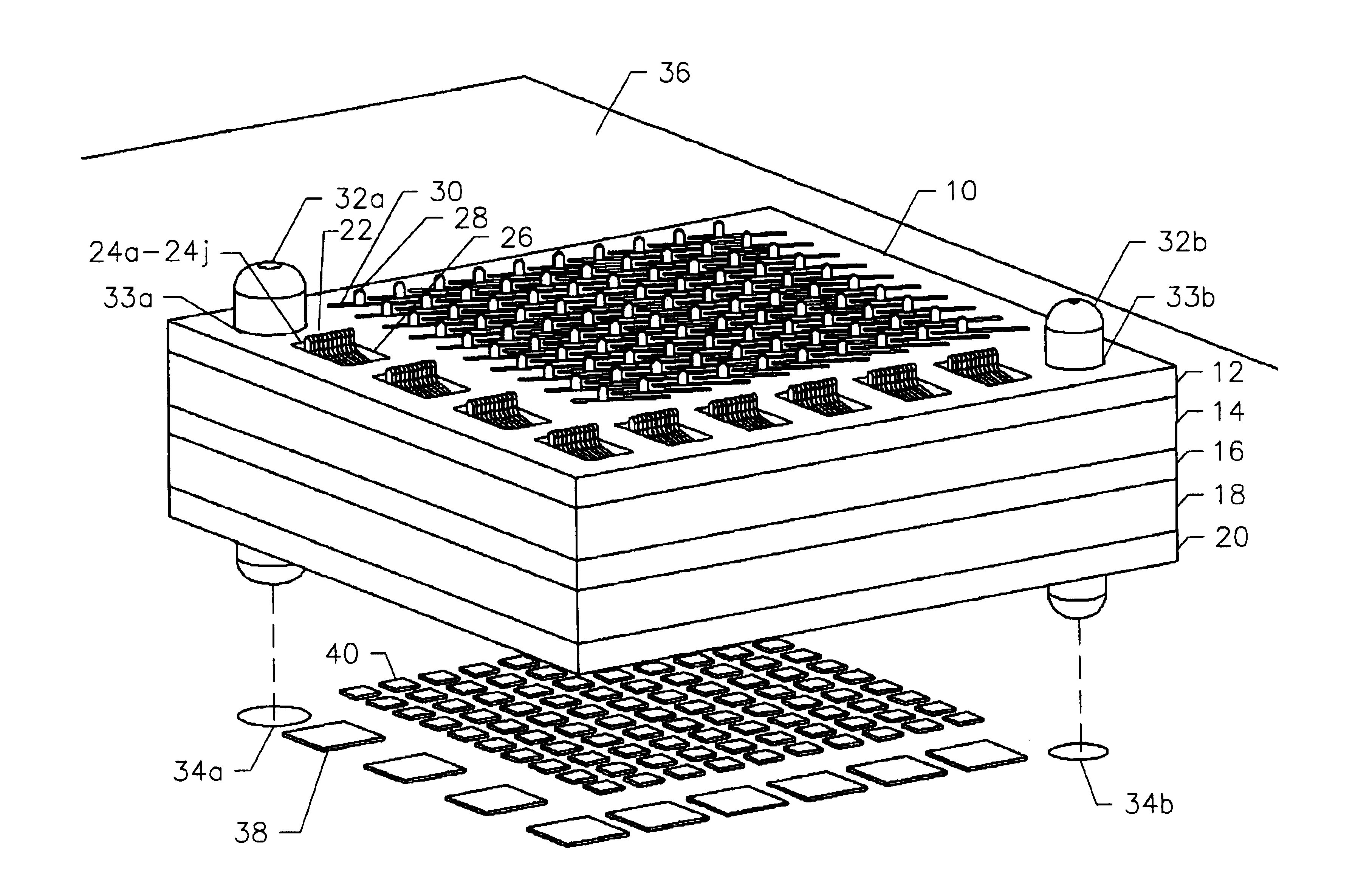
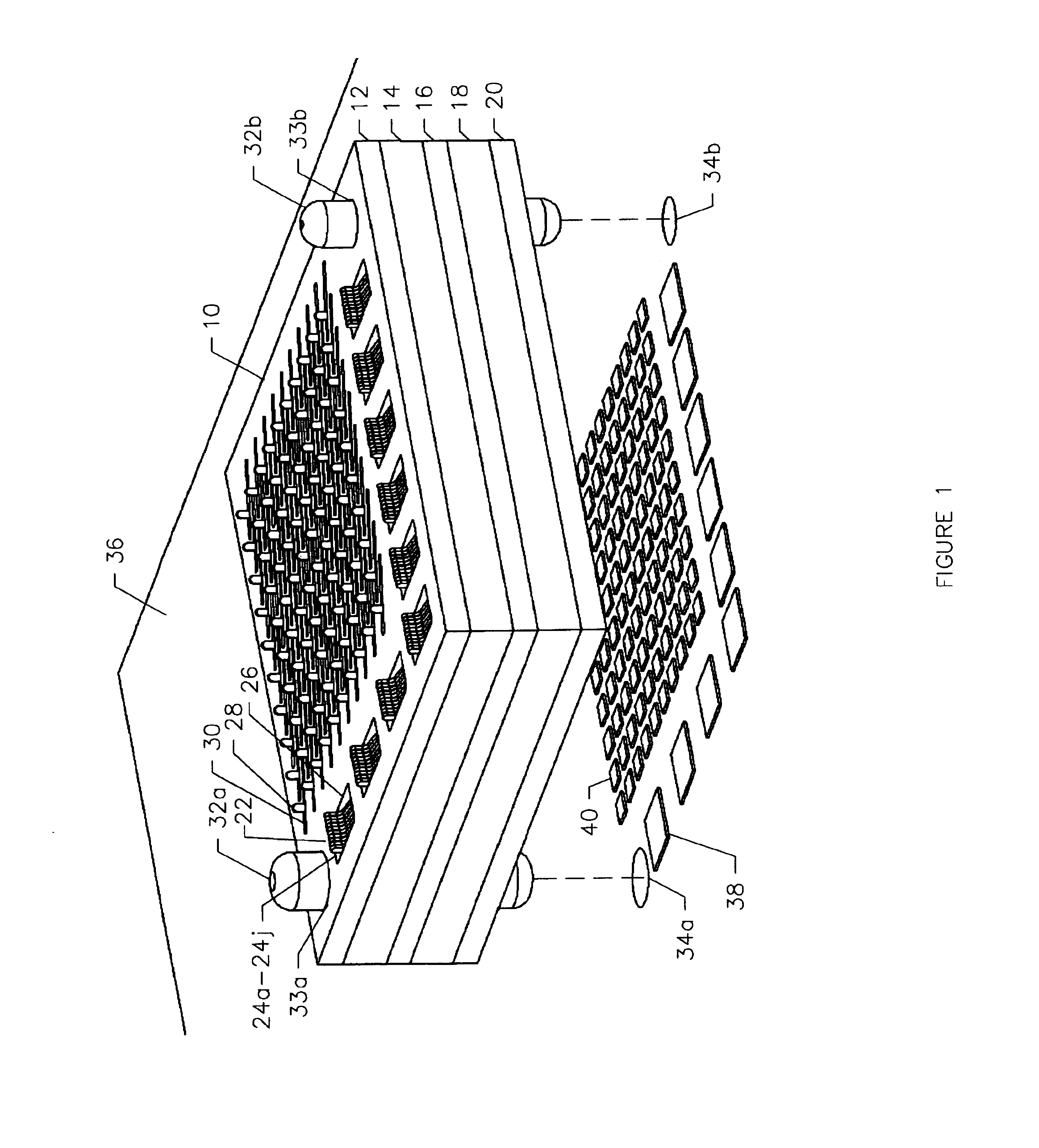
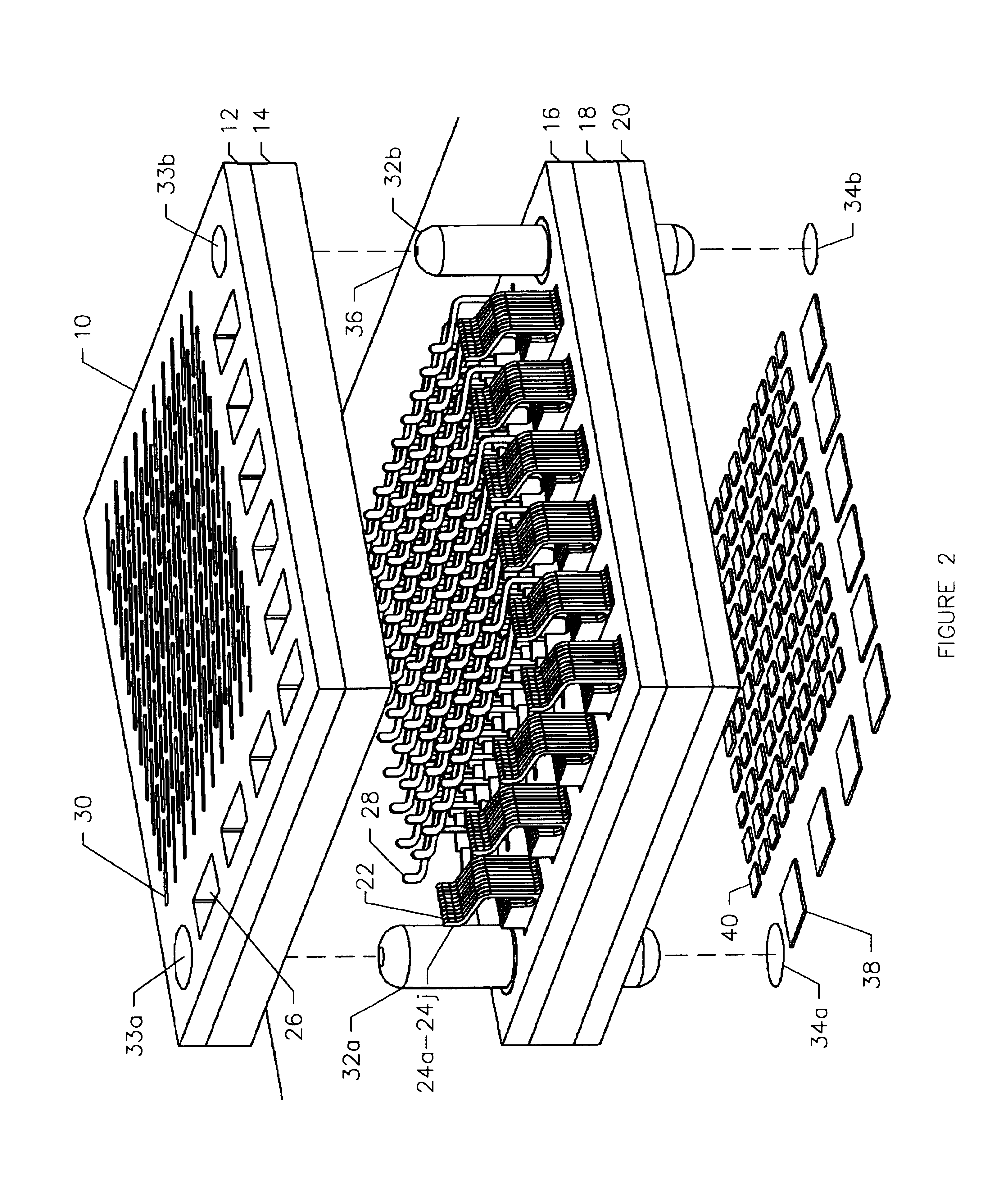
Reference is now made to the Drawings wherein like reference characters denote like or similar parts throughout the various Figures. Referring now to FIG. 1, a perspective view of an area array connector, generally designated as 10, in accordance with the present invention is illustrated. The area array connector 10 includes an interposer housing comprised of a number of generally planar laminated layers, for example five generally planar laminated layers. In an embodiment of the present invention, the first laminated layer 12, second laminated layer 14, third laminated layer 16, fourth laminated layer 18, and fifth laminated layer 20 are constructed of insulative materials such as plastics, ceramics, epoxy with glass filler, etc. The laminated layers 12, 14, 16, 18, and 20 are secured to one another using various suitable means, such as an adhesive.

In accordance with the principles of the present invention, at least one power interconnector 22, comprised of a number of electrical c...


PUM


Abstract

An area array connector adapted to connect contact pads on a first generally planar circuit element to corresponding contact pads on a second generally planar circuit element is described. The area array connector includes an interposer housing and at least one electrical interconnector positioned within the interposer housing. The at least one electrical interconnector is comprised of a plurality of electrical contacts stacked in a substantially parallel relationship to one another. The at least one electrical interconnector is positioned to make contact with a first contact pad on the first generally planar circuit element and a second contact pad on the second generally planar circuit element to provide an electrical interconnection therebetween.

Description

BACKGROUND OF THE INVENTION1. Technical Field of the InventionThe present invention is generally directed to area array connectors adapted to connect the contact pads of one generally planar circuit element, such as a printed circuit board, to corresponding contact pads on another generally planar circuit element.2. Description of Related ArtIn many electronic applications, compactness of the electronic assembly is an important goal. One manner of achieving this compactness is to stack circuit cards, such as printed circuit boards, one upon another, and electrically connecting the circuit cards together.In order to make use of such a compact arrangement, it is necessary that the face-to-face connection of circuit cards be made assuredly both electrically and mechanically. Interposers, such as area array connectors, are often used to connect corresponding contact pads on adjacent circuit cards for this purpose.An important component of many interposer designs for electrically connect...

Claims


Application Information

Patent Timeline
IPC IPC(8): H01R13/24H01R13/22H01R12/04
CPCH01R13/2435H01R12/714H01R12/52H01R12/73
Inventor GRANT, JOHN L.CUFF, MICHAEL P.
Owner AIRBORN
Learn More