Liquid crystal display device and fabricating method thereof

Inactive Publication Date: 2005-04-05
LG DISPLAY CO LTD
View PDF12 Cites 15 Cited by
  • Summary
  • Abstract
  • Description
  • Claims
  • Application Information

AI Technical Summary

Benefits of technology

Accordingly, it is an object of the present invention to provide a liquid crystal display, and a fabricating method thereof, having features that reduce picture quality degradation and / or short-circuiting between adjacent pixel electrodes.

Problems solved by technology

This can cause data signal deterioration, which results in degraded picture quality.

Method used


Image

  • Liquid crystal display device and fabricating method thereof
  • Liquid crystal display device and fabricating method thereof
  • Liquid crystal display device and fabricating method thereof

Examples


Embodiment Construction

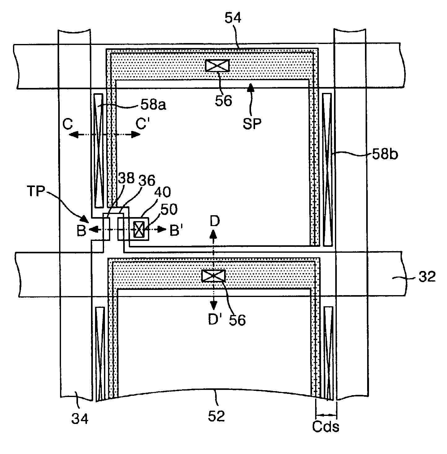
FIG. 5 and FIG. 6 illustrate a lower substrate of a liquid crystal display according to an embodiment of the present invention. Referring to FIG. 5 and FIG. 6, the lower substrate 31 of the liquid crystal display (LCD) includes a TFT TP at an intersection between a data line 34 and a gate line 32, a pixel electrode 52 that is connected to a drain electrode 40 of the TFT TP, and a storage capacitor SP that is positioned over part of a gate line 32.

The TFT TP includes a gate electrode 36 that is connected to the gate line 32, a source electrode 38 that is connected to the data line 34, and a drain electrode 40 that is connected, via a drain contact hole 50, to the pixel electrode 52. Further, the TFT TP includes semiconductor layers 44 and 46 that define a conductive channel between the source electrode 38 and the drain electrode 40 when a gate voltage is applied to the gate electrode 36. The TFT TP thus responds to gate signals on the gate line 32 to selectively apply data signals fr...


PUM


Abstract

A liquid crystal display device, and its fabrication method, having reduced picture quality deterioration and shorts. A thin film transistor is provided at intersections of gate and data lines. A pixel electrode connects to the thin film transistor. A storage electrode overlaps part of a gate line and extends along data lines. That storage electrode is overlapped by part of the pixel electrode. Channels are defined between the storage electrode and the data lines. A constant gap between the pixel electrodes and the data lines prevent a deterioration of picture quality and shorts between adjacent pixel electrodes and between the storage electrode and the data lines.

Description

This application claims the benefit of Korean Patent Application No. 2001-0081771, field on Dec. 20, 2001, which is hereby incorporated by reference.BACKGROUND OF THE INVENTION1. Field of the InventionThis invention relates to liquid crystal displays. More particularly, it relates to preventing picture quality deterioration and shorting between adjacent pixel electrodes.2. Description of the Related ArtA liquid crystal display (LCD) uses an electric field to control light transmittance to produce an image. An LCD includes a liquid crystal panel having a matrix of liquid crystal cells, and driving circuits for driving the liquid crystal cells. The liquid crystal panel includes a common electrode and pixel electrodes for producing electric fields in accordance with data signals. Typically, the pixel electrodes are provided on a lower substrate, whereas the common electrode is on an upper substrate. Usually, each pixel electrode is connected to a thin film transistor (TFT) that acts as...

Claims


Application Information

Patent Timeline
IPC IPC(8): G02F1/13G02F1/1362G02F1/136
CPCG02F1/136213G02F1/136
Inventor PARK, CHEOL WOOLEE, MIN JIC
Owner LG DISPLAY CO LTD
Why Eureka
Try Eureka